LM12896FCW-1
LCD Module User Manual
Prepared by:
Checked by:
Approved by:
Caiwei
Date: 2022-07-06
Date:
Date:
Rev.
Descriptions
Release Date
0.1
Prelimiay release
2020-07-09
0.2
Update SPI to default interface
2022-07-06
URL:
www.topwaydisplay.com
Document Name: LM12896FCW-1-Manual-Rev0.2.doc
Page: 1 of 18

TOPWAY
LCD Module User Manual
LM12896FCW-1
Table of Content
1. Basic Specifications
............................................................................................................3
1.1 Display Specifications ...................................................................................................................................................3
1.2 Mechanical Specifications
.....................................................................................................................................3
1.3 Block Diagram
...................................................................................................................................................3
1.4 Terminal Functions
...................................................................................................................................................4
1.5 Jumper Functions
...................................................................................................................................................4
2. Absolute Maximum Ratings
................................................................................................5
3. Electrical Characteristics
................................................................................................5
3.1 DC Characteristics
...................................................................................................................................................5
3.2 LED Backlight Circuit Characteristics
......................................................................................................................5
3.3 8080 Interface
...................................................................................................................................................6
3.4 6800 Interface
...................................................................................................................................................7
3.5 4-Line SPI MCU Interface
.....................................................................................................................................8
3.6 3-Line SPI MCU Interface
.....................................................................................................................................9
3.7 I2C MCU Interface
.................................................................................................................................................10
3.8 Reset Timing ...............................................................................................................................................................10
4. Function Specifications ..........................................................................................................11
4.1 Adjusting the Display Contrast ........... .......................................................................................................................11
4.2 Resetting the LCD module
...................................................................................................................................11
4.3 Power off the LCD Module
...................................................................................................................................11
4.4 Refreshing The LCD Module
...................................................................................................................................11
4.5 Display Memory Map .................................................................................................................................................11
4.6 Display Data RAM (DDRAM)
...................................................................................................................................12
4.7 Instructions ...............................................................................................................................................................13
Design and Handling Precaution ..............................................................................................17
URL:
www.topwaydisplay.com
Document Name: LM12896FCW-1-Manual-Rev0.2.doc
Page: 2 of 18
TOPWAY
LCD Module User Manual
LM12896FCW-1
1. Basic Specifications
1.1
Display Specifications
1) LCD Display Mode
: FSTN, Positive, Transflective
2) Display Color
: Display Data = “1” : Dark Gray (*1)
: Display Data = “0” : Light Gray (*2)
3) Viewing Angle
: 6 H
4) Driving Method
: 1/96 duty, 1/10bias
5) Back Light
: White LED backlight
Note:
*1. Color tone may slightly change by Temperature and Driving Condition.
*2. The Color is defined as the inactive / background color
*3. Fine Contrast adjustment function is necessary in application design for optimal display result
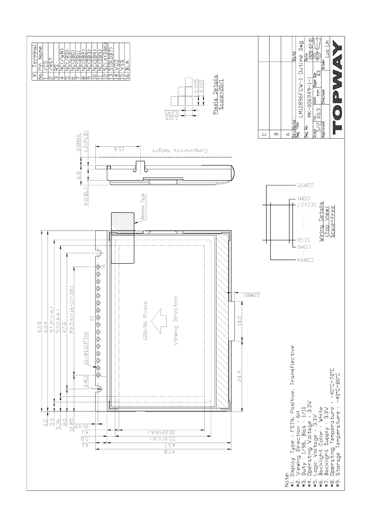
1.2
Mechanical Specifications
1) Outline Dimension
: 63.8 x 47.8 x 9.8MAX
(see attached Outline Drawing for details)
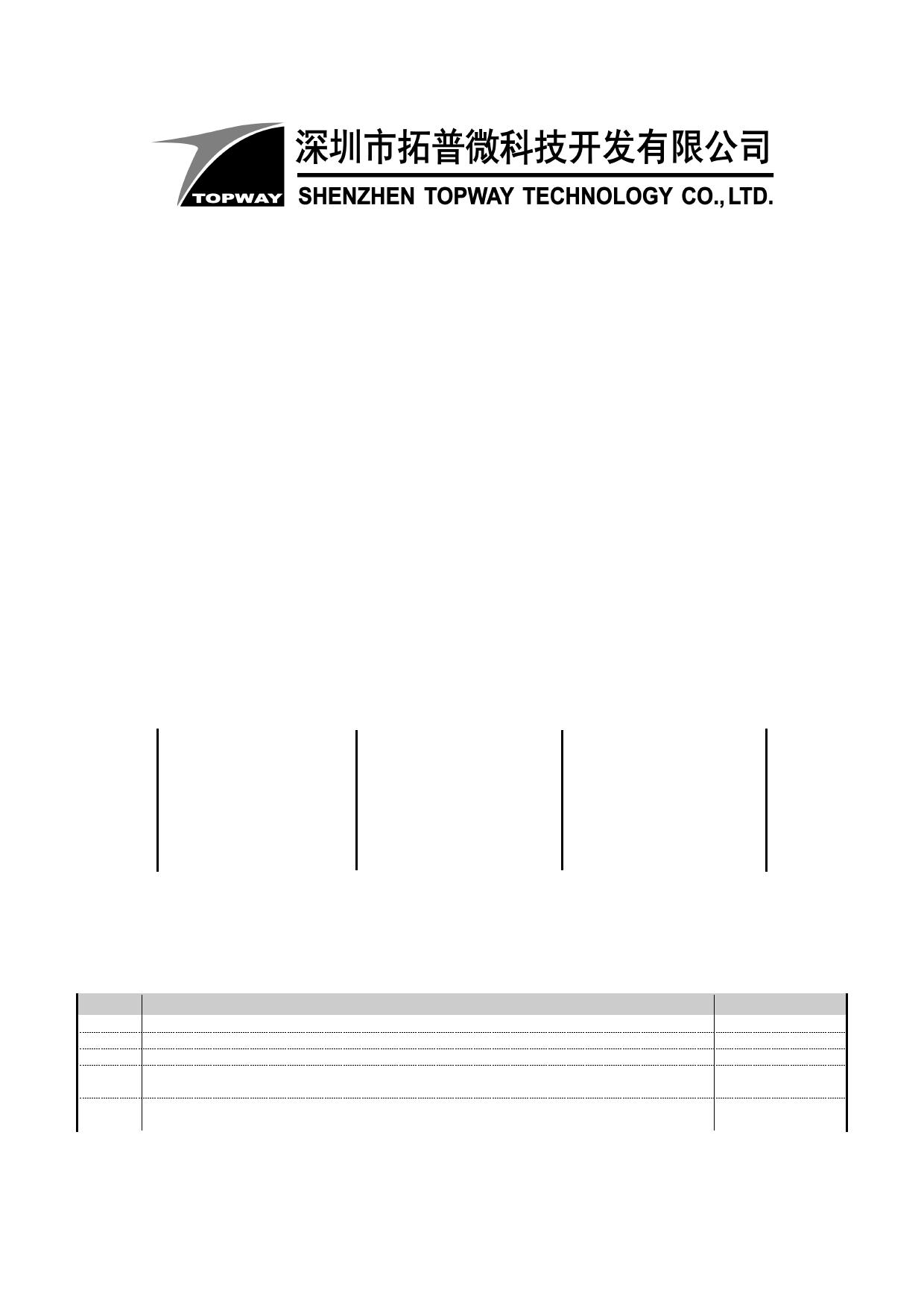
1.3
Block Diagram
BLA
LED
Backlight Circuit
LCD Panel
128 x 96 pixels
VDD
VSS
/CS,/RST,RS,(/WR),(/RD),
ST75161 or equivalent
(DB0~,DB5),SCLK(DB6),SID(DB7)
URL:
www.topwaydisplay.com
Document Name: LM12896FCW-1-Manual-Rev0.2.doc
Page: 3 of 18
TOPWAY
LCD Module User Manual
LM12896FCW-1
1.4
Terminal Functions
Pin No.
Descriptions
Pin
8-bit
I/O
K1,K2 K3
Name
8-bit parallel
parallel
4-pin
3-pin
I2C serial
8080 mode
6800
SPI(default)
SPI
interface
mode
Chip select input pin.
/CS=“L”: This chip is selected and the MPU interface is
1
1
/CS
Input
active.
Connect to VSS
/CS=“H”: This chip is not selected and the MPU interface
is disabled(DB7~DB0] are high impedance).
Reset signal.
2
2
/RST
Input
/RST = L, internal Initialization is executed.
/RST = H, Normal running.
Register Select
3
3
RS
Input
RS = H, Transferring the Display RAM data
Connect to VDD
RS = L, Transferring the Instruction data
/WR=L H,
R/W = H,
/RD=H;
E=L;
Data or
Data or
4
-
NC(/WR)
Input
Instruction
Status
latch into the
read form
LCD module
the LCD
module
Not used,
leave open or pull Hi
/WR=H, /RD=L;
R/W=L,
Data or Status
E= H L;
5
-
NC(/RD)
Input
read form the
Data or
LCD module
Instruction
latch into
the LCD
module
6
-
NC(DB0)
I/O
7
-
NC(DB1)
I/O
8
-
NC(DB2)
I/O
No connect, leave open.
8-bit Data bus;
9
-
NC(DB3)
I/O
Three state I/O terminal for
10
-
NC(DB4)
I/O
display data or instruction
11
-
NC(DB5)
I/O
data When /CS=H,
Connect to VDD
12
4 SCLK(DB6) I/O
DB0~DB7= High
serial input clock (SCL)
Impedance
SDA_IN, serial input data
13
5
SID(DB7)
I/O
SDA_OUT, serial data and acknowledge
output for the I2C interface.
14
6
VDD
Power
Positive Power Supply
15
7
VSS
Power
Negative Power Supply, Ground (0V)
16
8
BLA
Power
Positive Power for LED backlight
1.5
Jumper Functions
Jumper Setting
Function Descriptions
OPEN
COLSE
JP1~JP10,JP13~JP15,JP18,JP20
JP11,JP12,JP16,JP17,JP19,JP21
Set to 8080 mode (8-bit parallel)
JP1~JP11,JP13,JP15,JP18,JP20
JP12,JP14,JP16,JP17,JP19,JP21
Set to 6800 interface mode (8-bit parallel)
JP10~JP13,JP19,JP21
JP1~JP9,JP14~JP18,JP20
Set to 4-pin SPI mode (serial)-default
JP11,JP12,JP16,JP19,JP21
JP1~JP10,JP13~JP15,JP17,JP18,JP20
Set to 3-pin SPI mode (serial)
JP12~JP14,JP19,JP21
JP1~JP11,JP15~JP18,JP20, C11 install 0R
Set I2C serial interface
URL:
www.topwaydisplay.com
Document Name: LM12896FCW-1-Manual-Rev0.2.doc
Page: 4 of 18
TOPWAY
LCD Module User Manual
LM12896FCW-1
2. Absolute Maximum Ratings
Items
Symbol
Min.
Max.
Unit
Condition
Supply Voltage
V DD
-0.3
4.0
V
V SS = 0V
Operating Temperature
T OP
-40
70
C
No Condensation
Storage Temperature
T ST
-40
80
C
No Condensation
Cautions:
Any Stresses exceeding the Absolute Maximum Ratings may cause substantial damage to the device. Functional
operation of this device at other conditions beyond those listed in the specification is not implied and prolonged exposure
to extreme conditions may affect device reliability.
3. Electrical Characteristics
3.1
DC Characteristics
V SS = 0V, V DD = 3.3V, T OP = 25 C
Items
Symbol
MIN.
TYP.
MAX.
Unit
Applicable Pin
Operating Voltage
V DD
3.0
3.3
3.6
V
VDD
Input High Voltage
V IH
0.7V DD
-
V DD
V
/CS, /RST, RS,
/WR(R/W), /RD(E),DB4-
Input Low Voltage
V IL
V SS
-
0.3V DD
V
DB7, DB0(SCLK), DB1~
DB3 (SID)
Output High Voltage
V OH
0.8V DD
-
V DD
V
Output Low Voltage
V OL
V SS
-
0.2V DD
V
DB0-DB7
Operating Current
I DD
-
0.89
3.13
mA
VDD
3.2
LED Backlight Circuit Characteristics
V SS = 0V, BLA = 3.3V, T OP = 25 C
Items
Symbol
MIN.
TYP.
MAX.
Unit
Applicable Pin
Forward Voltage
BLA
-
3.3
-
V
BLA
Forward Current
I BLA
-
48
60
mA
BLA
Cautions:
Exceeding the recommended driving current could cause substantial damage to the backlight and shorten its lifetime.
BLA
VS
NO.of LEDs = 3 pcs
URL:
www.topwaydisplay.com
Document Name: LM12896FCW-1-Manual-Rev0.2.doc
Page: 5 of 18
TOPWAY
LCD Module User Manual
LM12896FCW-1
3.3
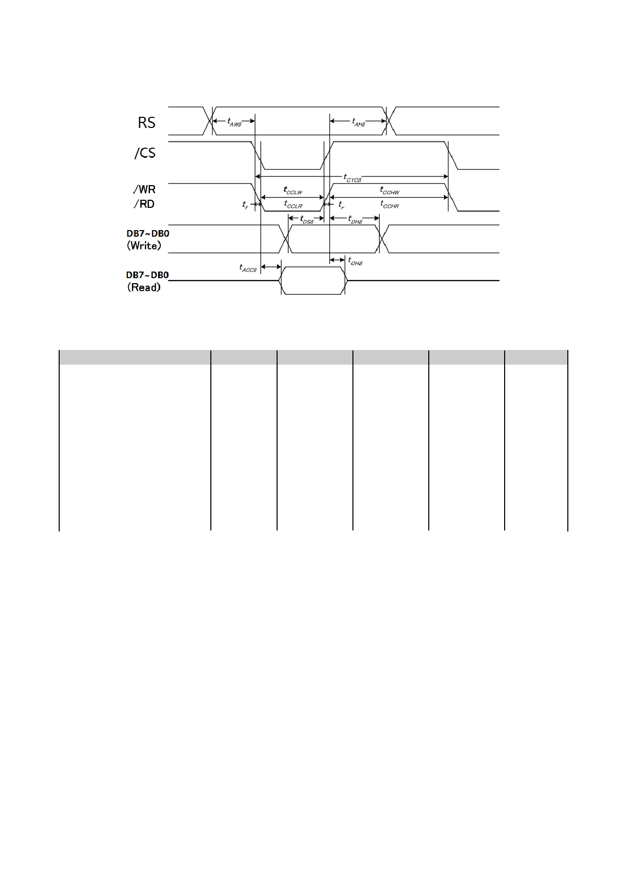
8080 Interface
8080 Interface Timing Diagram
V SS = 0V, V DD = 3.3V, T OP = 25 C
Item
Symbol
MIN.
TYP.
MAX.
Unit
Address Setup Time
tAW8
26
-
-
ns
Address Hold Time
tAH8
0
-
-
ns
System cycle time(WRITE)
tCYC8
208
-
-
ns
/WR L pulse width(WRITE)
tCCLW
91
-
-
ns
/WR H pulsewidth(WRITE)
tCCHW
91
-
-
ns
System cycle time (READ)
tCYC8
520
-
-
ns
/RD L pulse width (READ)
tCCLR
234
-
-
ns
WRITE Data setup time
tCCHR
234
-
-
ns
WRITE Data hold time
tDS8
19.5
-
-
ns
Output Disable Time
tDH8
19.5
-
-
ns
READ access time
tACC8
-
130
ns
READ Output disable time
tOH8
13
77
ns
note: signal rise time and fall time should less than 15ns.
URL:
www.topwaydisplay.com
Document Name: LM12896FCW-1-Manual-Rev0.2.doc
Page: 6 of 18
TOPWAY
LCD Module User Manual
LM12896FCW-1
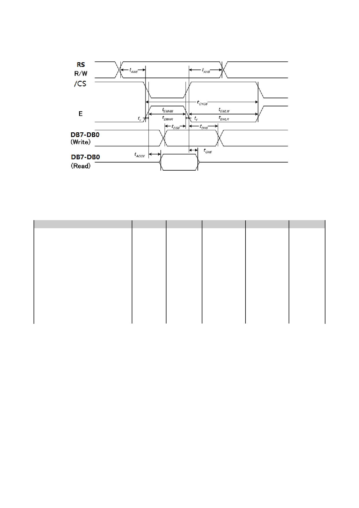
3.4
6800 Interface
6800 Interface Timing Diagram
V SS = 0V, V DD = 3.3V, T OP = 25 C
Item
Symbol
MIN.
TYP.
MAX.
Unit
Address Setup Time
tAW6
26
-
-
ns
Address Hold Time
tAH6
0
-
-
ns
System cycle time(WRITE)
tCYC6
208
-
-
ns
Enable L pulse width(WRITE)
tEWLW
91
-
-
ns
Enable H pulse width(WRITE)
tEWHW
91
-
-
ns
System cycle time (READ)
tCYC6
520
-
-
ns
Enable L pulse width (READ)
tEWLR
234
-
-
ns
Enable H pulse width (READ)
tEWHR
234
-
-
ns
Write data setup time
tDS6
19.5
-
-
ns
Write data hold time
tDH6
19.5
-
-
ns
Read data access time
tACC6
-
130
ns
Read data output disable time
tOH6
13
77
ns
note: signal rise time and fall time should less than 15ns.
URL:
www.topwaydisplay.com
Document Name: LM12896FCW-1-Manual-Rev0.2.doc
Page: 7 of 18
TOPWAY
LCD Module User Manual
LM12896FCW-1
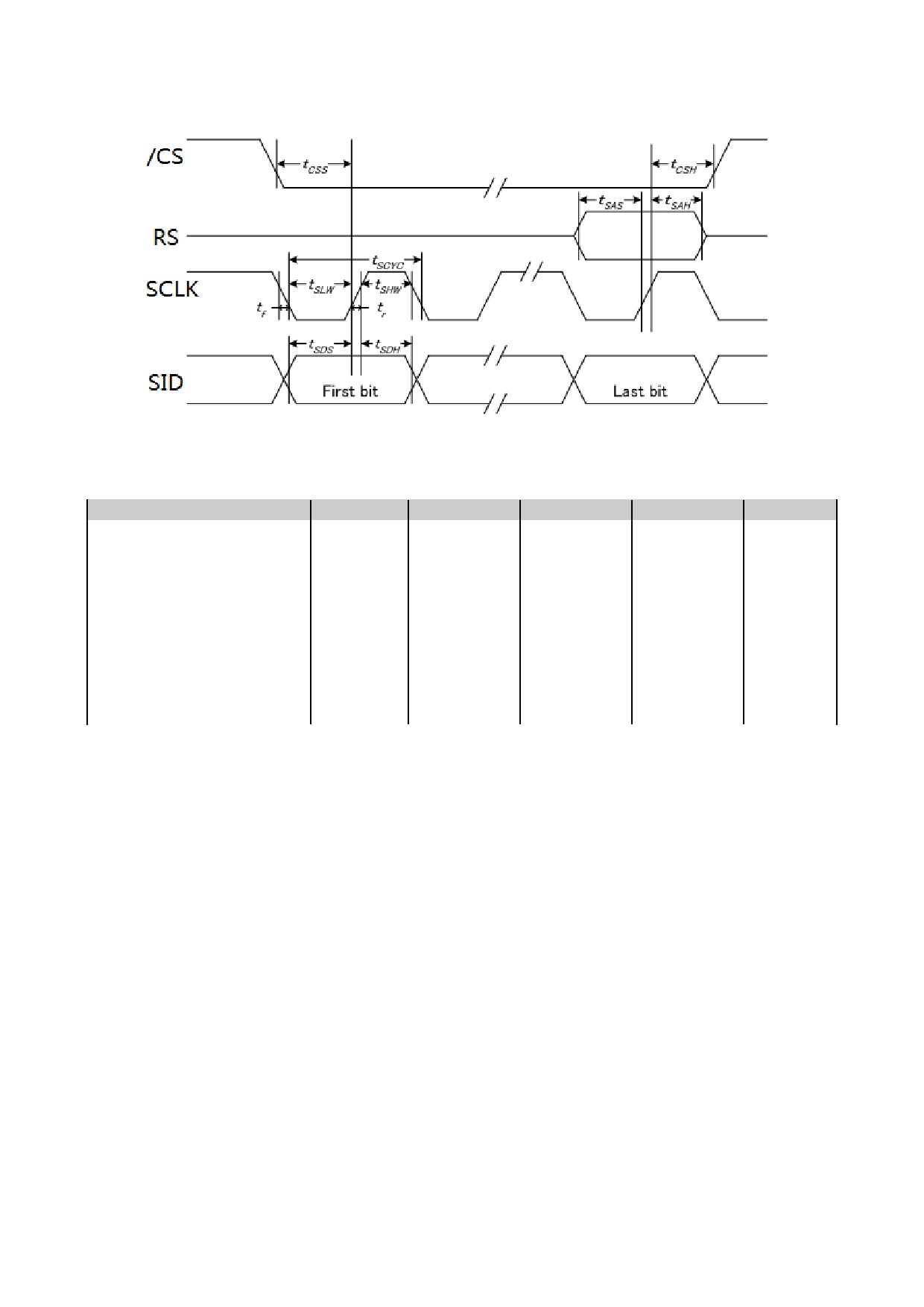
3.5
4-Line SPI MCU Interface
4-Line S PI Interface Timing Diagram
V SS = 0V, V DD = 3.3V, T OP = 25 C
Item
Symbol
MIN.
TYP.
MAX.
Unit
Serial clock period
tSCYC
104
-
-
ns
SCL “H” pulse width
tSHW
39
-
-
ns
SCL “L” pulse width
tSLW
39
-
-
ns
Address setup time
tSAS
26
-
-
ns
Address hold time
tSAH
26
-
-
ns
Data setup time
tSDS
26
-
-
ns
Data hold time
tSDH
26
-
-
ns
CSB-SCLK time
tCSS
26
-
-
ns
CSB-SCLK time
tCSH
26
-
-
ns
CS “H” pulse width
tCHW
0
-
-
ns
note: signal rise time and fall time should less than 15ns
URL:
www.topwaydisplay.com
Document Name: LM12896FCW-1-Manual-Rev0.2.doc
Page: 8 of 18
TOPWAY
LCD Module User Manual
LM12896FCW-1
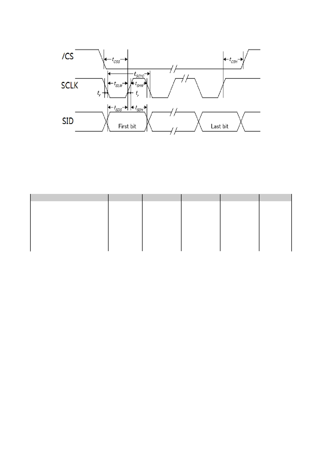
3.6
3-Line SPI MCU Interface
3-Line S PI Interface Timing Diagram
V SS = 0V, V DD = 3.3V, T OP = 25 C
Item
Symbol
MIN.
TYP.
MAX.
Unit
Serial clock period
tSCYC
104
-
-
ns
SCL “H” pulse width
tSHW
39
-
-
ns
SCL “L” pulse width
tSLW
39
-
-
ns
Data setup time
tSDS
26
-
-
ns
Data hold time
tSDH
26
-
-
ns
CSB-SCL time
tCSS
26
-
-
ns
CSB-SCL time
tCSH
26
-
-
ns
note: signal rise time and fall time should less than 15ns
URL:
www.topwaydisplay.com
Document Name: LM12896FCW-1-Manual-Rev0.2.doc
Page: 9 of 18
TOPWAY
LCD Module User Manual
LM12896FCW-1
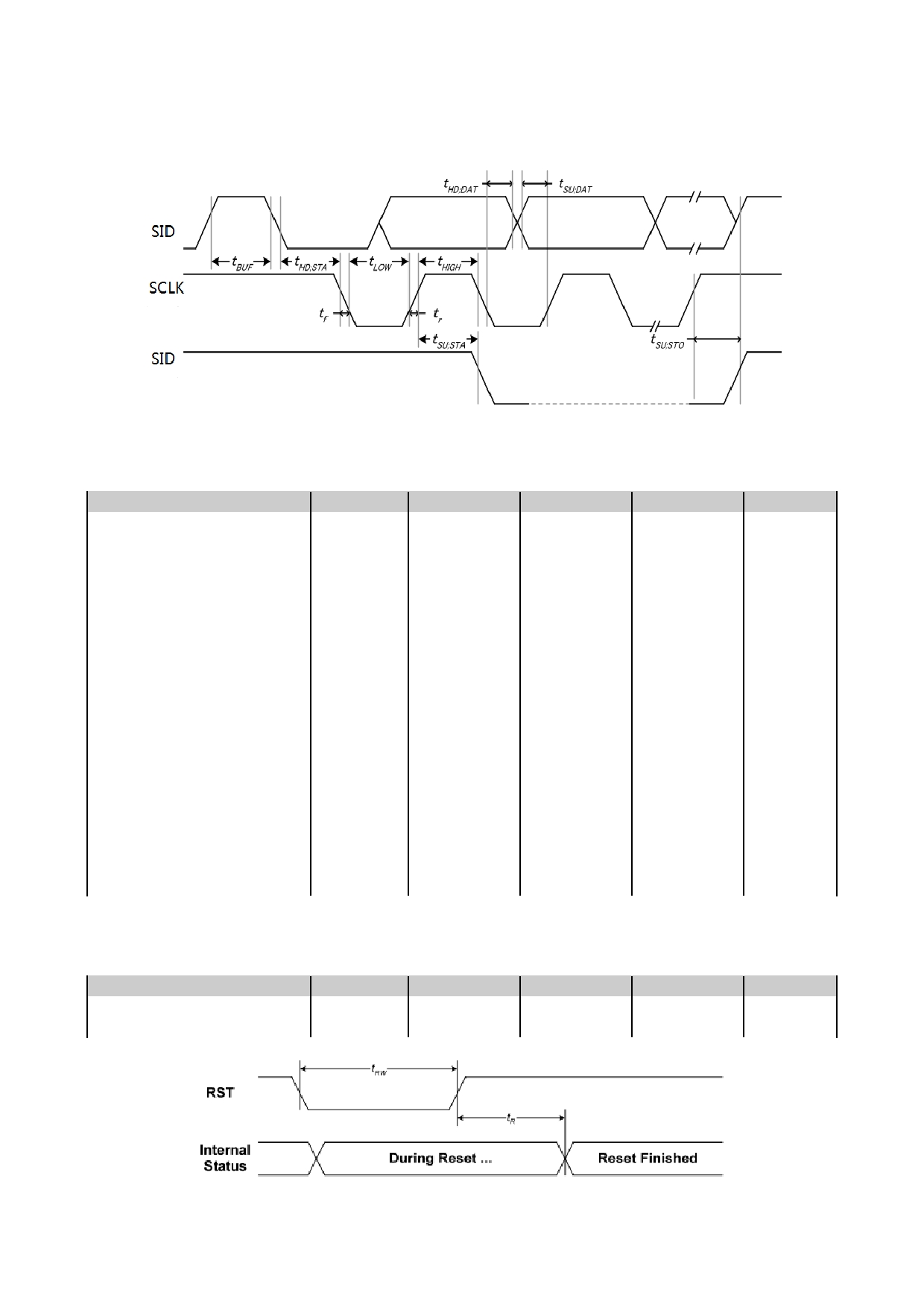
3.7
I2C MCU Interface
I2C Interface Timing Diagram
V SS = 0V, V DD = 3.3V, T OP = 25 C
Item
Symbol
MIN.
TYP.
MAX.
Unit
SCL clock frequency
fSCL
-
-
400
KHZ
SCL clock low period
tLOW
1.69
-
-
us
SCL clock high period
tHIGH
0.78
-
-
us
Data set-up time
tSU;Data
1.3
-
-
us
Data hold time
tHD;Data
0
-
0.63
us
Setup time for a repeated
START condition
tSU;STA
0.78
-
-
us
Start condition hold time
tHD;STA
0.78
-
-
us
Setup time for STOP
condition
tSU;STO
0.78
-
-
us
Bus free time between a
STOP and START
tBUF
1.3
-
-
us
Signal rise time
tr
26+0.1Cb
-
210
ns
Signal fall time
tf
26+0.1Cb
-
210
ns
Capacitive load
represented by each bus
Cb
-
-
400
pF
line
Tolerable spike width on
bus
tSW
-
-
35
ns
note: signal rise time and fall time should less than 15ns
3.8
Reset Timing
V SS =0V, V DD =3.3V, T OP =25 C
Item
Symbol
MIN.
TYP.
MAX.
Unit
Reset time
tR
-
-
1-
ms
Reset “L” pulse width
tRW
1
-
-
ms
Reset Timing Diagram
URL:
www.topwaydisplay.com
Document Name: LM12896FCW-1-Manual-Rev0.2.doc
Page: 10 of 18
TOPWAY
LCD Module User Manual
LM12896FCW-1
4. Function Specifications
4.1
Adjusting the Display Contrast
-- This LCD module equipped with latest digital contrast adjustment function.
-- Its display contrast could be adjusted by MCU command. (Please see the command tables
for details)
-- It is recommended to provide a contrast adjustment interface for end-user, where the best
display result could meet the individual preference in mass production.
4.2
Resetting the LCD module
The LCD module should be initialized by setting /RST terminal at low level after the power supply
stable.
4.3
Power off the LCD Module
It recommends that LCD module should enter sleep mode before power off.
4.4
Refreshing The LCD Module
It recommends that the operating modes and display contents should be refreshed periodically to
prevent the effect of unexpected noise.
4.5
Display Memory Map
Page
Address
Data
LCD Module Top View
D7
0
:
D0
D7
1
:
D0
:
:
D7
5
:
128x96 pixels
D0
:
:
D7
8
:
D0
:
:
D7
11
:
D0
Column Address
00h
7F
Internal Display RAM Address
Note:
Display start line = 0,INV = 0.
URL:
www.topwaydisplay.com
Document Name: LM12896FCW-1-Manual-Rev0.2.doc
Page: 11 of 18
TOPWAY
LCD Module User Manual
LM12896FCW-1
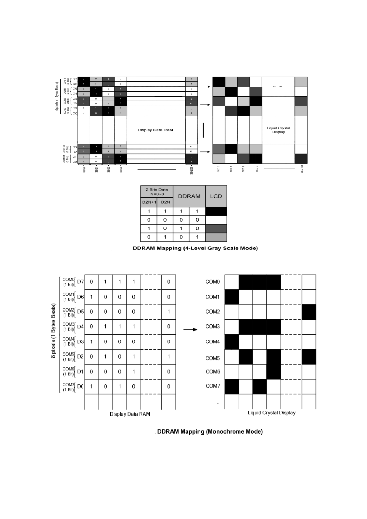
4.6
Display Data RAM (DDRAM)
URL:
www.topwaydisplay.com
Document Name: LM12896FCW-1-Manual-Rev0.2.doc
Page: 12 of 18
TOPWAY
LCD Module User Manual
LM12896FCW-1
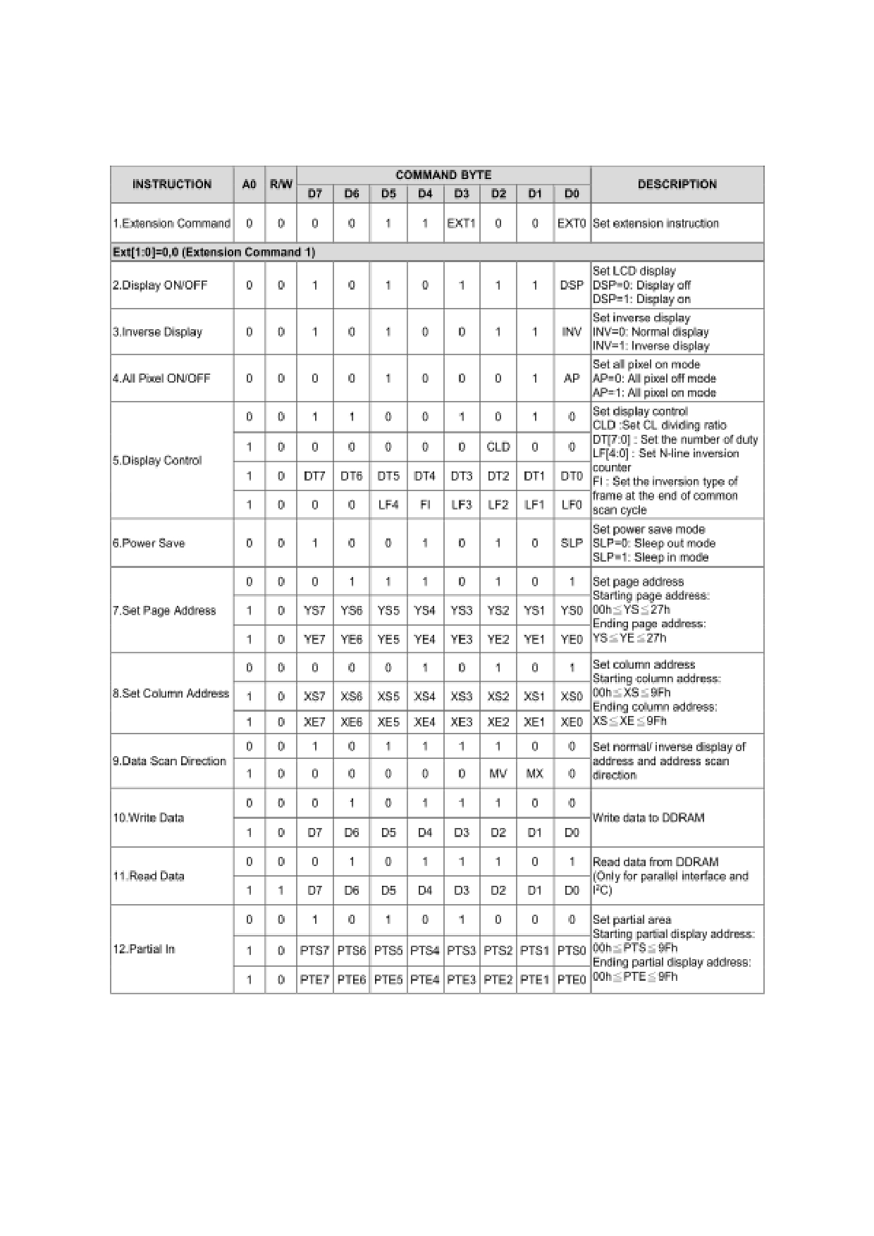
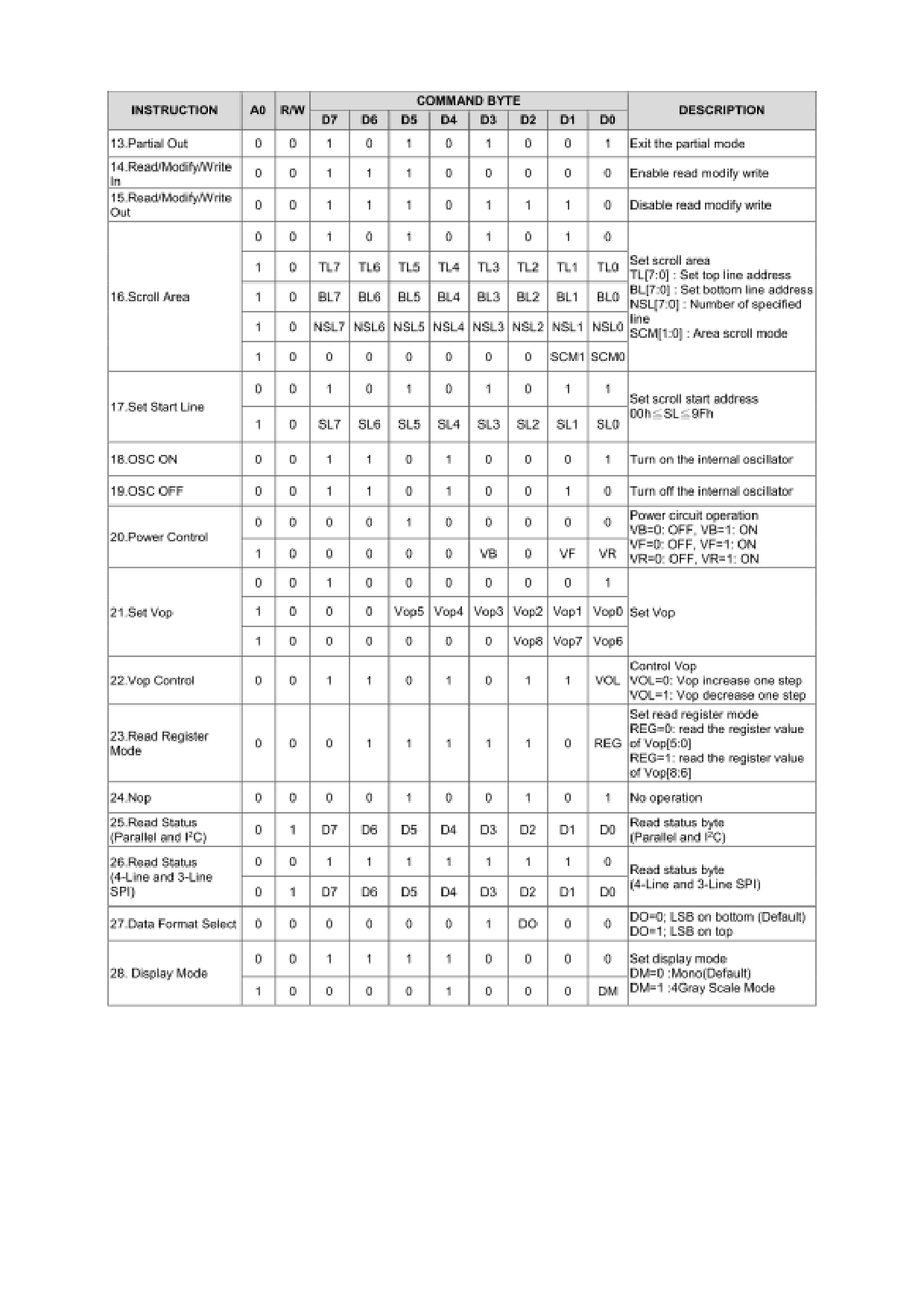
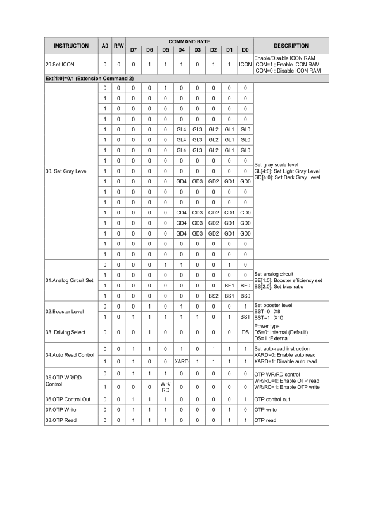
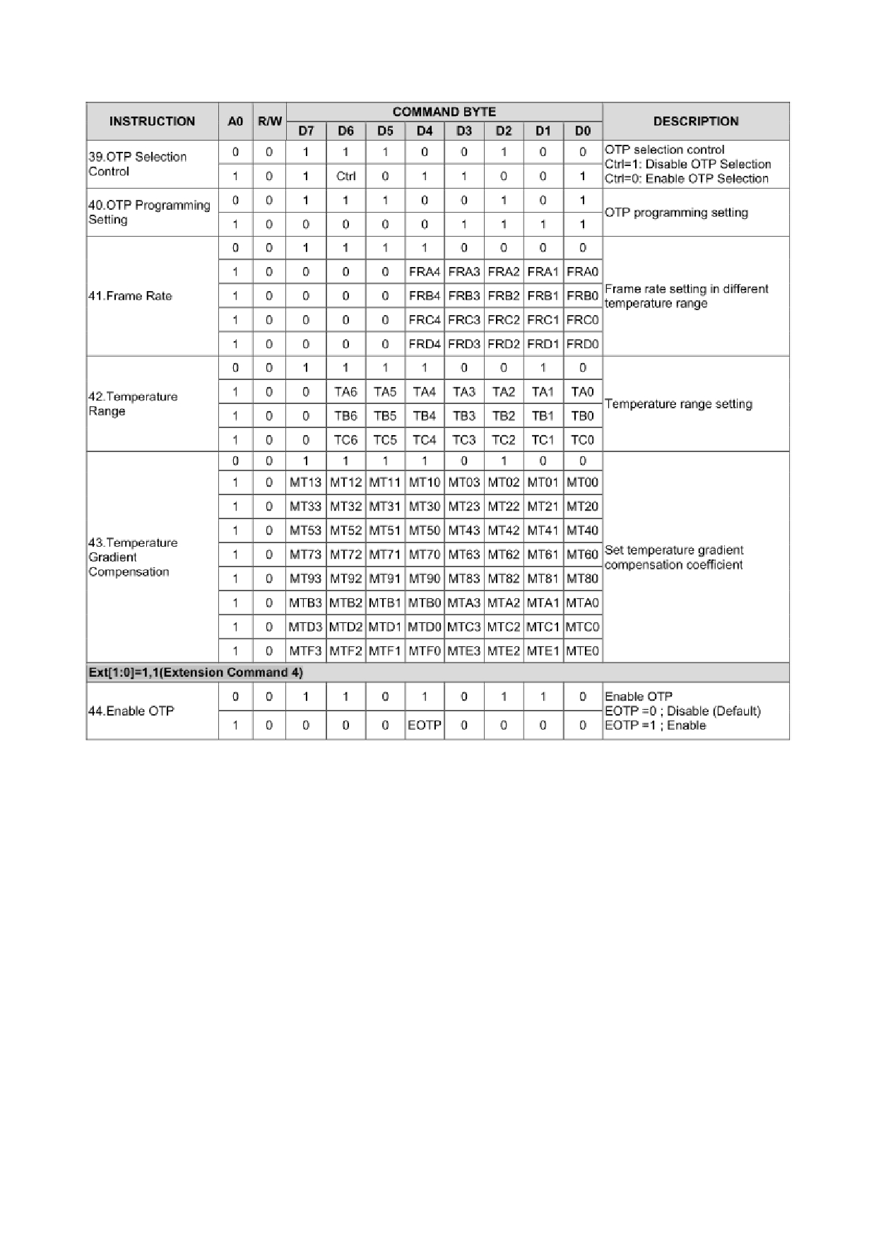
4.7
Instructions
URL:
www.topwaydisplay.com
Document Name: LM12896FCW-1-Manual-Rev0.2.doc
Page: 13 of 18
TOPWAY
LCD Module User Manual
LM12896FCW-1
URL:
www.topwaydisplay.com
Document Name: LM12896FCW-1-Manual-Rev0.2.doc
Page: 14 of 18
TOPWAY
LCD Module User Manual
LM12896FCW-1
URL:
www.topwaydisplay.com
Document Name: LM12896FCW-1-Manual-Rev0.2.doc
Page: 15 of 18
TOPWAY
LCD Module User Manual
LM12896FCW-1
Note:
*1. Do not use any other command not listed, or the system malfunction may result.
*2. For the details of the Display Commands, please refer to ST75161 data sheet.
URL:
www.topwaydisplay.com
Document Name: LM12896FCW-1-Manual-Rev0.2.doc
Page: 16 of 18

TOPWAY
LCD Module User Manual
LM12896FCW-1
Design and Handling Precaution
1.
The LCD panel is made by glass. Any mechanical shock (eg. dropping form high place)
will damage the LCD module.
2.
Do not add excessive force on the surface of the display, which may cause the Display
color change abnormally.
3.
The polarizer on the LCD is easily get scratched. If possible, do not remove the LCD
protective film until the last step of installation.
4.
Never attempt to disassemble or rework the LCD module.
5.
Only Clean the LCD with Isopropyl Alcohol or Ethyl Alcohol. Other solvents (eg. water)
may damage the LCD.
6.
When mounting the LCD module, make sure that it is free form twisting, warping and
distortion.
7.
Ensure to provide enough space (with cushion) between case and LCD panel to
prevent external force adding on it, or it may cause damage to the LCD or degrade the
display result.
8.
Only hold the LCD module by its side. Never hold LCD module by add force on the heat
seal or TAB.
9.
Never add force to component of the LCD module. It may cause invisible damage or
degrade of the reliability.
10.
LCD module could be easily damaged by static electricity. Be careful to maintain an
optimum anti-static work environment to protect the LCD module.
11.
When peeling off the protective film from LCD, static charge may cause abnormal
display pattern. It is normal and will resume to normal in a short while.
12.
Take care and prevent get hurt by the LCD panel sharp edge.
13.
Never operate the LCD module exceed the absolute maximum ratings.
14.
Keep the signal line as short as possible to prevent noisy signal applying to LCD
module.
15.
Never apply signal to the LCD module without power supply.
16.
IC chip (eg. TAB or COG) is sensitive to the light. Strong lighting environment could
possibly cause malfunction. Light sealing structure casing is recommend.
17.
LCD module reliability may be reduced by temperature shock.
18.
When storing the LCD module, avoid exposure to the direct sunlight, high humidity, high
temperature or low temperature. They may damage or degrade the LCD module.
URL:
www.topwaydisplay.com
Document Name: LM12896FCW-1-Manual-Rev0.2.doc
Page: 17 of 18
TOPWAY
LCD Module User Manual
LM12896FCW-1
URL:
www.topwaydisplay.com
Document Name: LM12896FCW-1-Manual-Rev0.2.doc
Page: 18 of 18