LM24080BCW-3
LCD Module User Manual
Prepared by:
Checked by:
Approved by:
Liuweilin
Date: 2012-04-07
Date:
Date:
Rev. Descriptions
Release Date
0.1
New release
2010-04-01
0.2
Revise Backlight power supply on 3.2 LED Backlight Circuit
2010-04-16
0.3
Update Interfacing Setting
2012-04-07
URL: www.topwaydisplay.com
Document Name:LM24080BCW-3-Manual-Rev0.3
Page: 1 of 9

TOPWAY
LCD Module User Manual
LM24080BCW-3
Table of Content
1. Basic Specifications .............................................................................................................. 3
1.1
Display Specifications 3
1.2
Mechanical Specifications
3
1.3
Block Diagram 3
1.4
Terminal Functions 4
2. Absolute Maximum Ratings .................................................................................................. 5
3. Electrical Characteristics ...................................................................................................... 5
3.1
DC Characteristics 5
3.2
LED Backlight Circuit Characteristics 5
3.3
AC Characteristics
6
3.4
Reset Timing 6
4. Function Specifications ......................................................................................................... 7
4.1
Resetting the LCD module 7
4.2
Interfacing Setting
7
4.3
Display Pixel Map(example) 7
4.4
Control Data and Command 8
4.5
Command Summary 8
5. Design and Handling Precaution .......................................................................................... 9
URL: www.topwaydisplay.com
Document Name:LM24080BCW-3-Manual-Rev0.3
Page: 2 of 9
TOPWAY
LCD Module User Manual
LM24080BCW-3
1. Basic Specifications
1.1 Display Specifications
1) LCD Display Mode
: FSTN, Positive, Transflective
2) Display Color
: Display Data = “1” : Dark Gray (*1)
: Display Data = “0” : Light Gray (*2)
3) Viewing Angle
: 6H
4) Driving Method
: 1/80 duty, 1/10 bias
5) Backlight
: White LED backlight
Note:
*1. Color tone may slightly change by Temperature and Driving Condition.
*2. The Color is defined as the inactive / background color
1.2 Mechanical Specifications
1) Outline Dimension
: 130.0 x 65.0 x 11.5 MAX.(Exclude FFC Terminal)
see attached Outline Drawing for details
1.3 Block Diagram
BLA
VSS
Backlight Circuit
240 x 80 pixels
LCD Panel
VDD
VSS
E,R/W,D/C, /CS0,/RST
UC1698
DB2~DB7
or equivalent
DB0(SCK)
DB1(SDA)
URL: www.topwaydisplay.com
Document Name:LM24080BCW-3-Manual-Rev0.3
Page: 3 of 9

TOPWAY
LCD Module User Manual
LM24080BCW-3
1.4 Terminal Functions
Descriptions
Pin
Pin
Display
No.
Name
I/O
8-bit parallel
8-bit parallel
Serial
68mode
80mode
4wire
3wire
1
VSS
Power
0V Power Supply, GND
2
VDD
Power
Positive Power Supply
3
NC
-
No connection,leave open
4
D/C
Input
Register Select
pull
D/C=HIGH: data on DB0 to DB7 is display data
down
D/C=LOW: data on DB0 to DB7 is command data
5
R/W
Input
In read mode
Write enable
pull down
R/W = H; Data read form LCD
input, active LOW
module, data appears
at DB0
– DB7 and can be read by the host
while, E = H and the device is
being selected
In write mode
R/W = L; Data write to the LCD
6
E
Input
module, data appears at DB0 –
DB7 will be written into the LCD
Read enable
module
input, active LOW
at E = H L and device is being
selected
7
DB0
IO
8-bit bi-directional data bus
Serial clock input
8
DB1
Serial data input
9
DB2
IO
pull up or pull
10
DB3
IO
down
11
DB4
IO
:
:
14
DB7
15
/CS0
Input
Chip Select Signal
/CS0=L: Data IO is enabled
16
/RST
Input
Reset Signal:
/RST = L, Reset the LCD Module
/RST = H, Normal Running
17
NC
-
No connection,leave open
18
NC
-
No connection,leave open
19
NC
-
No connection,leave open
20
BLA
Power
Positive Power Supply for LED backlight
note:
*1. The LCM Fixed to 68 mode by default ,could been changed to serial and 80 mode by
changing jumpers
URL: www.topwaydisplay.com
Document Name:LM24080BCW-3-Manual-Rev0.3
Page: 4 of 9
TOPWAY
LCD Module User Manual
LM24080BCW-3
2. Absolute Maximum Ratings
Items
Symbol
Min.
Max.
Unit
Condition
Supply Voltage
V DD
-0.3
+3.6
V
V SS = 0V
Input Voltage
V IN
-0.3
V DD +0.3
V
V SS = 0V
Operating Temperature
T OP
-20
+70
C
No Condensation
Storage Temperature
T ST
-30
+80
C
No Condensation
Cautions:
Any Stresses exceeding the Absolute Maximum Ratings may cause substantial damage to the device. Functional operation of this
device at other conditions beyond those listed in the specification is not implied and prolonged exposure to extreme conditions may
affect device reliability.
3. Electrical Characteristics
3.1 DC Characteristics
V SS =0V, V DD =3.0V, T OP =25 C
Items
Symbol
MIN.
TYP.
MAX.
Unit Applicable Pin
Operating Voltage
V DD
2.7
3.0
3.3
V
VDD
DB0~DB7, E, R/W,/CS0,
Input High Voltage
V IN
0.7xVDD
-
VDD
V
D/C, /RST,
DB0~DB7, E, R/W,/CS0,
Input Low Voltage
V IN
VSS
-
0.2xVDD
V
D/C, /RST
Operating Current
I DD
-
0.6
2.3
mA VDD
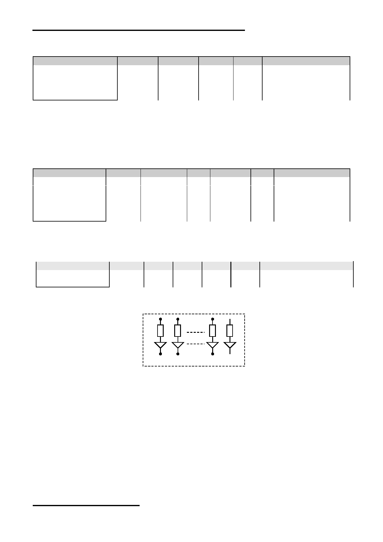
3.2 LED Backlight Circuit Characteristics
BLK=0V, If BLA =102mA, T OP =25 C
Items
Symbol
MIN.
TYP.
MAX.
Unit
Applicable Pin
Forward Voltage
Vf BLA
-
3.3
-
V
BLA
Forward Current
If BLA
-
102
120
mA
BLA
Cautions:
Exceeding the recommended driving current could cause substantial damage to the backlight and shorten its lifetime.
BLA
BLK
No. of LED = 6 pcs
URL: www.topwaydisplay.com
Document Name:LM24080BCW-3-Manual-Rev0.3
Page: 5 of 9
TOPWAY
LCD Module User Manual
LM24080BCW-3
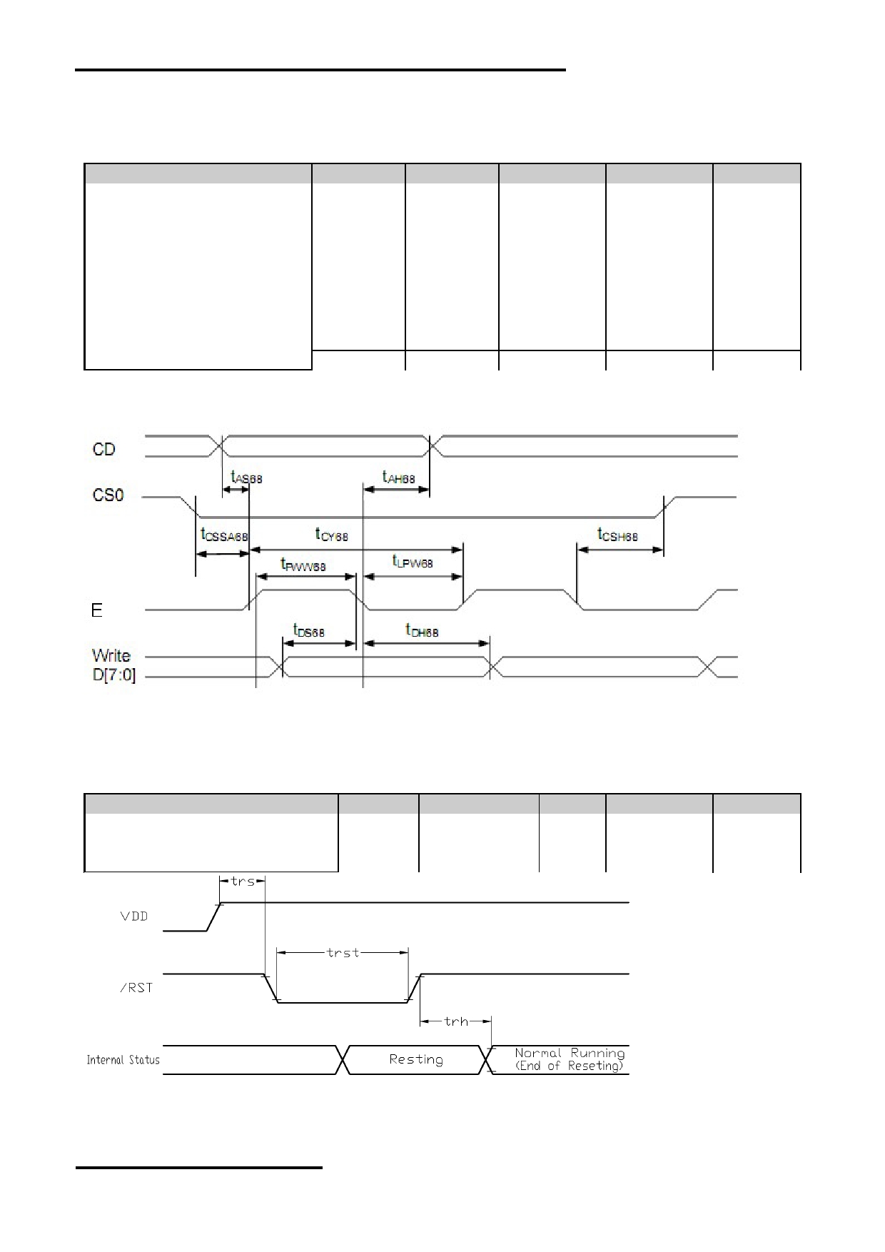
3.3 AC Characteristics
3.3.1 68 Mode
V SS =0V, V DD =3.0V, T OP =25 C
Item
Symbol
MIN.
TYP.
MAX.
Unit
Address setup time
tAS68
0
-
-
ns
Address hold time
tAH68
0
-
-
ns
System cycle time
tCY68
80
-
-
ns
Pulse width
tPWW68
50
-
-
ns
Low pulse width
tLPW68
40
-
-
ns
Data setup time
tDS68
30
-
-
ns
Data hold time
tDH68
0
-
-
ns
tCSSA68
Chip select setup time
5
-
-
ns
tCSH68
5
-
-
ns
Note: *1. Input signal rise/fall time should be less than 20ns
For details, please refer to UC1698U datasheet.
Bus Timing Diagram
3.4 Reset Timing
V SS =0V, V DD =3.0V, T OP =25 C
Item
Symbol
MIN.
TYP.
MAX.
Unit
Reset setup time
trs
1.0
-
-
ms
Reset hold time
trh
1.0
-
-
ms
Reset active time
trst
150
-
-
us
Reset Timing Diagram
URL: www.topwaydisplay.com
Document Name:LM24080BCW-3-Manual-Rev0.3
Page: 6 of 9
TOPWAY
LCD Module User Manual
LM24080BCW-3
4. Function Specifications
4.1 Resetting the LCD module
The LCD module should be initialized by hardware reset, using /RST terminal.
While turning on the VDD and VSS power supply, maintain /RST terminal at LOW level. After the
power supply stabilized, release the reset terminal (/RST=HIGH)
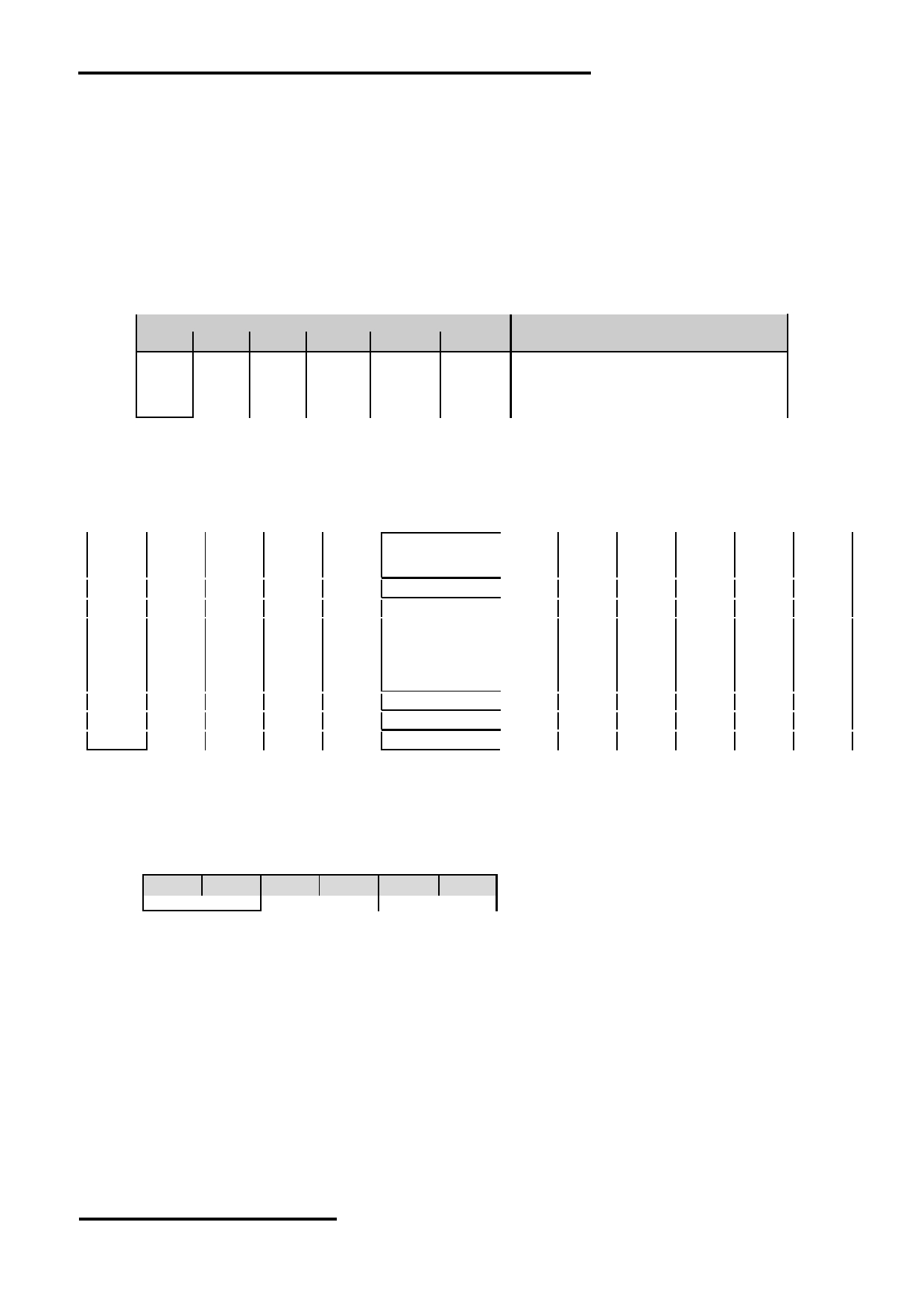
4.2 Interfacing Setting
Jumpers could been used to change bus interfacing family
Jumpers
JP1
JP2
JP3
JP4
JP5
JP6
Function Discription
open close close open
close
open
68 mode 8 bit selected <default>
open close open close close
open
80 mode 8 bit selected
close open open close open
close
4wire serial *1
NOTE 1: In serial mode, the pin E must been pull down,and other unused control pins and data bus pins been connected to VDD or
VSS
4.3 Display Pixel Map(example)
1,1
2,1
3,1
4,1
5,1
- - -
- - -
236,1
237,1
238,1
239,1
240,1
1,2
2,2
3,2
4,2
5,2
- - -
- - -
236,2
237,2
238,2
239,2
240, 2
1,3
2,3
3,3
4,3
5,3
- - -
- - -
236,3
237,3
238,3
239,3
240, 3
:
:
:
:
:
:
:
:
:
:
:
:
:
:
:
:
:
:
:
:
:
:
:
:
:
:
:
:
:
:
:
:
:
:
:
:
1, 78
2, 78
3, 78
4, 78
5, 78
- - -
- - -
236,238 237, 78 238, 78 239, 78
240,78
1, 79
2, 79
3, 79
4, 79
5, 79
- - -
- - -
236, 79 237, 79 238, 79 239, 79
240,79
1, 80
2, 80
3, 80
4, 80
5, 80
- - -
- - -
236, 80 237, 80 238, 80 239, 80
240,80
Pixel mapping (Top View)
Note:
*1.
Based on the top view of the LCD module,
the 1, 1 (x, y) pixel is the upper-left pixel;
the 240, 80 (x, y) pixel is the lower-right pixel.
*2.
The registet LC[7:6] is set to 01b.
*3
1,1
2,1
3,1
4,1
5,1
6,1
1st byte
2nd byte
3rd byte
Pixel[1,1]=1st byte D7~D4,Pixel[2,1]=1st byte D3~D0,Pixel[3,1]=2nd byte D7~D4, Pixel[4,1]=2nd byte D3~D0.
*4.
For the details of memory mapping please refer to UC1698 datasheet.
URL: www.topwaydisplay.com
Document Name:LM24080BCW-3-Manual-Rev0.3
Page: 7 of 9

TOPWAY
LCD Module User Manual
LM24080BCW-3
4.4 Control Data and Command
The LCD module setting is controlled by the internal Register Values.
The Register Address should be addressed when RS=1 and Register Value should be issued when RS=0.
A full command sequence should be as follow.
Steps
E
RS
Data (DB0~ DB7)
1 st
H L
1
Register Address
2 nd
H L
0
Register Value
4.5 Command Summary
Note: *1.For the details, please refer to UC1698 Data sheet.
*2. C/D: 0:Control, 1:Data; W/R: 0: Write Cycle, 1:Read Cycle(Read available in 68 mode); #: Useful Data bIts; - Don’t Care
URL: www.topwaydisplay.com
Document Name:LM24080BCW-3-Manual-Rev0.3
Page: 8 of 9

TOPWAY
LCD Module User Manual
LM24080BCW-3
5. Design and Handling Precaution
Please refer to "LCD-Module-Design-Handling-Precaution.pdf".
URL: www.topwaydisplay.com
Document Name:LM24080BCW-3-Manual-Rev0.3
Page: 9 of 9