
LM3033DDW-0B
LCD Module User Manual
Shenzhen TOPWAY Technology Co., Ltd.
Rev. Descriptions
Release Date
0.1
Preliminary New release
2007-12-18
URL: www.topwaydisplay.com
Document Name: LM3033DDW-0B-Manual-Rev0.1
Page: 1 of 13

TOPWAY
LCD Module User Manual
LM3033DDW-0B
Table of Content
1. Basic Specifications .............................................................................................................. 3
1.1
Display Specifications ............................................................................................................................................ 3
1.2
Mechanical Specifications ...................................................................................................................................... 3
1.3
Block Diagram ........................................................................................................................................................ 3
1.4
Terminal Functions ................................................................................................................................................. 4
2. Absolute Maximum Ratings .................................................................................................. 5
3. Electrical Characteristics ...................................................................................................... 5
3.1
DC Characteristics ................................................................................................................................................. 5
3.2
LED Backlight Circuit Characteristics ..................................................................................................................... 5
3.3
AC Characteristics (Parallel Mode Interface) ......................................................................................................... 6
3.4
AC Characteristics (Serial Mode Interface) ............................................................................................................ 7
3.5
Reset Timing .......................................................................................................................................................... 7
4. Function Specifications ......................................................................................................... 8
4.1
Resetting the LCD module ..................................................................................................................................... 8
4.2
Using Parallel interface .......................................................................................................................................... 8
4.3
Using Serial interface ............................................................................................................................................. 8
4.4
Display Memory Map ............................................................................................................................................. 9
4.5
Display Control Instructions ................................................................................................................................. 11
5. Design and Handling Precaution ........................................................................................ 13
URL: www.topwaydisplay.com
Document Name: LM3033DDW-0B-Manual-Rev0.1
Page: 2 of 13
TOPWAY
LCD Module User Manual
LM3033DDW-0B
1. Basic Specifications
1.1 Display Specifications
1) LCD Display Mode
: STN-GRAY, Positive, Transflective
2) Display Color
: Display Data = “1” : Deep Blue(*1)
: Display Data = “0” : Light Gray(*2)
3) Viewing Angle
: 6 H
4) Driving Method
: 1/33 duty, 1/5bias
5) Back Light
: White LED backlight
Note:
*1. Color tone may slightly change by Temperature and Driving Condition
*2. The Color is defined as the inactive / background color
1.2 Mechanical Specifications
1) Outline Dimension
: 93.0 x 70.0 x 12.1MAX
(see attached Outline Drawing for details)
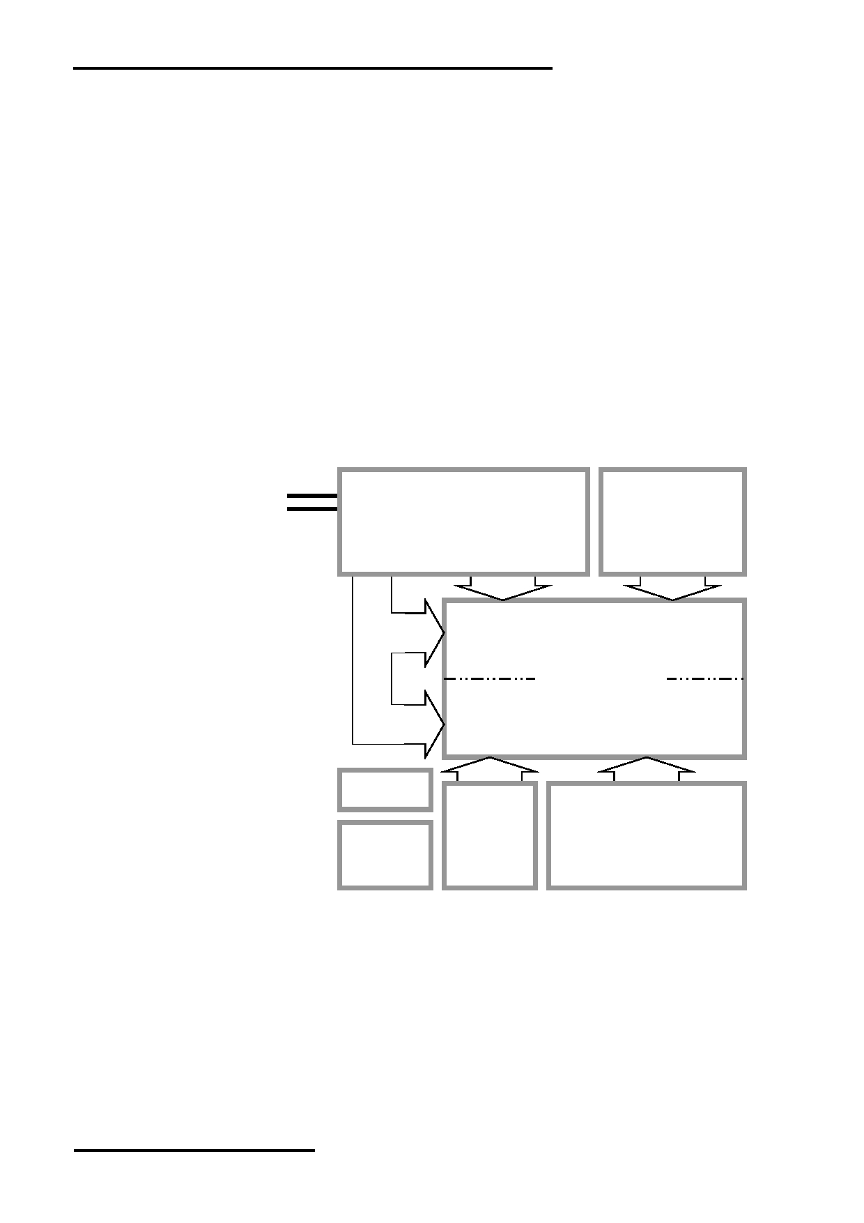
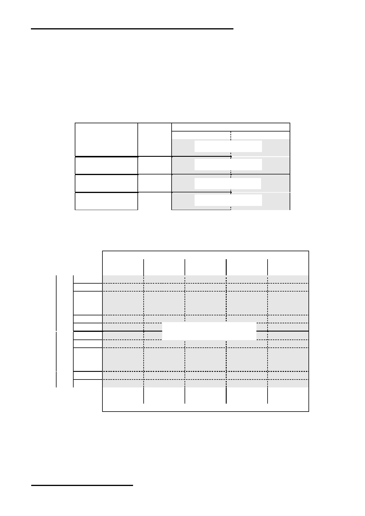
1.3 Block Diagram
DB0 - DB7
ST7920
ST7921 (2/3)
RS(CS), R/W(SID), E(SCLK)
or
or
equivalent
equivalent
/RST
PSB
LCD Panel
128 x 64 pixels
BLA
LED BL
BLK
Circuit
VDD
Power
ST7921 (1/3)
ST7921
VSS
Circuit
or
or
equivalent
equivalent
URL: www.topwaydisplay.com
Document Name: LM3033DDW-0B-Manual-Rev0.1
Page: 3 of 13

TOPWAY
LCD Module User Manual
LM3033DDW-0B
1.4 Terminal Functions
Pin
Pin
Descriptions
No. Name
I/O
Parallel mode (PSB=H)
Serial Mode (PSB=L)
1
VSS
Power Negative Power Supply, Ground (0V)
2
VDD
Power Positive Power Supply
3
NC
-
No Connection (keep open)
4
RS
Input Register Select
Chip Select (*1)
(CS)
RS=H; data read or write
CS=H, enable the data transfer.
RS=L; Instruction data write or
CS=L, reset the serial data counter
status busy flag read
R/W
Input Read write control
Chip Select
5
(SID)
R/W=H; data or status read
SID=serial data line
R/W=L; data or command write
6
E
Input E=Enable trigger
SCLK=Serial Clock
(SCLK)
7
DB0
I/O
Three state I/O terminal for display In serial mode,
:
:
:
data or instruction data
these terminal could leave open or
14
DB7
I/O
In 4 bit mode, DB3~DB0 could
pull-up
leave open or pull-up
15
PSB
Input Interface selection:
PSB=L; serial mode
PSB=H; 8 or 4 bit parallel bus mode
16
NC
-
No Connection (keep open)
17
/RST
Input System reset; low active
18
NC
-
No Connection (keep open)
19
BLA
Power Positive Power for LED backlight
20
BLK
Power Negative Power for LED backlight
Note:
*1. In serial mode, the CS is for resetting the serial data shifting counter,
It could not disable the data shifting into the LCD module.
URL: www.topwaydisplay.com
Document Name: LM3033DDW-0B-Manual-Rev0.1
Page: 4 of 13
TOPWAY
LCD Module User Manual
LM3033DDW-0B
2. Absolute Maximum Ratings
Items
Symbol
Min.
Max.
Unit
Condition
Supply Voltage
V DD
-0.3
5.5
V
V SS = 0V
Input Voltage
V IN
-0.3
V DD +0.3
V
V SS = 0V
Operating Temperature
T OP
-20
70
C
No Condensation
Storage Temperature
T ST
-30
80
C
No Condensation
Cautions:
Any Stresses exceeding the Absolute Maximum Ratings may cause substantial damage to the device. Functional operation of this
device at other conditions beyond those listed in the specification is not implied and prolonged exposure to extreme conditions may
affect device reliability.
3. Electrical Characteristics
3.1 DC Characteristics
V SS =0V, V DD =5.0V, T OP =25 C
Items
Symbol
MIN.
TYP.
MAX.
Unit
Applicable Pin
Operating Voltage
V DD
4.8
5.0
5.2
V
VDD
Input High Voltage
V IH1
0.8V DD
-
V DD
V
RS, R/W, E, PSB, /RST,
Input Low Voltage
V IL1
V SS
-
0.4
V
DB0-DB7
Output High Voltage
V OH1
0.7V DD
-
V DD
V
DB0-DB7 (I OH = -0.1mA)
Output Low Voltage
V OL1
V SS
-
0.6
V
DB0-DB7 (I OL = 0.1mA)
Operating Current
I DD
-
2.3
5.5
mA
VDD, VSS
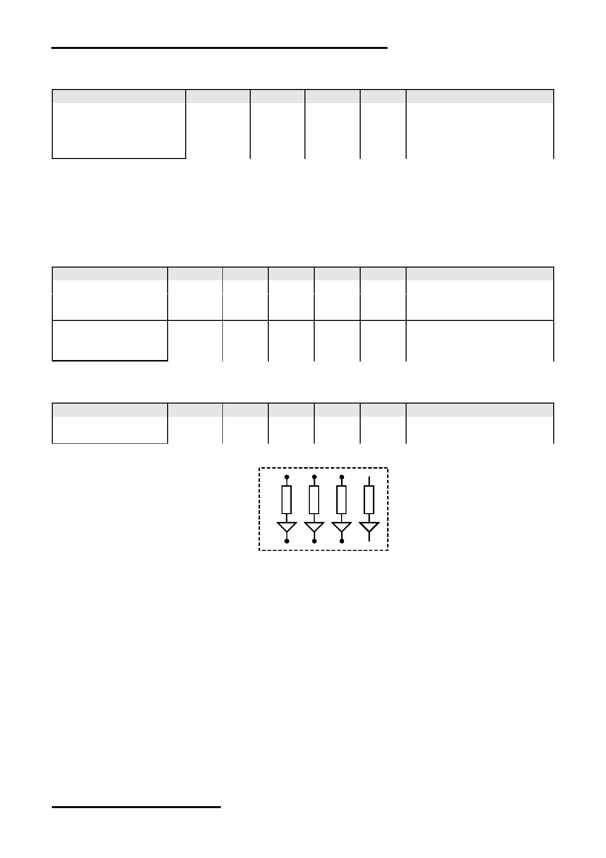
3.2 LED Backlight Circuit Characteristics
BLK=0V, If BLA =80mA, T OP =25 C
Items
Symbol
MIN.
TYP.
MAX.
Unit
Applicable Pin
Forward Voltage
Vf A
-
5.0
-
V
BLA
Forward Current
If A
-
80
100
mA
BLA
Cautions:
Exceeding the recommended driving current could cause substantial damage to the backlight and shorten its lifetime.
BLA
BLK
URL: www.topwaydisplay.com
Document Name: LM3033DDW-0B-Manual-Rev0.1
Page: 5 of 13
TOPWAY
LCD Module User Manual
LM3033DDW-0B
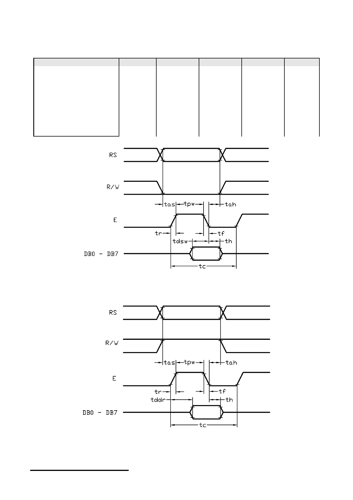
3.3 AC Characteristics (Parallel Mode Interface)
V SS =0V, V DD =5V, T OP =25 C
Item
Symbol
MIN.
TYP.
MAX.
Unit
E cycle time
tc
1500
-
-
ns
E high level width
tpw
175
-
-
ns
E rise time
tr
-
-
20
ns
E fall time
tf
-
-
20
ns
Address set-up time
tas
13
-
-
ns
Address hold time
tah
25
-
-
ns
Data set-up time
tdsw
50
-
-
ns
Data delay time
tddr
-
-
125
ns
Data hold time
th
25
-
-
ns
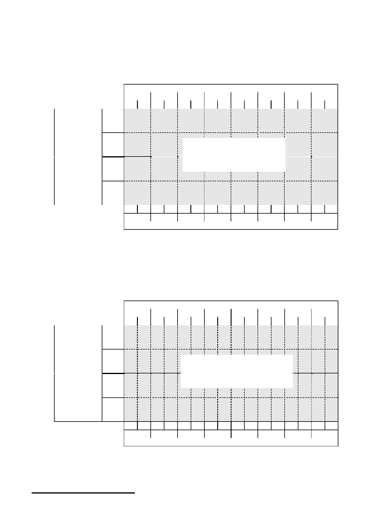
Host Write Timing Diagram (Parallel Mode)
Host Read Timing Diagram (Parallel Mode)
URL: www.topwaydisplay.com
Document Name: LM3033DDW-0B-Manual-Rev0.1
Page: 6 of 13

TOPWAY
LCD Module User Manual
LM3033DDW-0B
3.4 AC Characteristics (Serial Mode Interface)
V SS =0V, V DD =5V, T OP =25 C
Item
Symbol
MIN.
TYP.
MAX.
Unit
Clock Cycle
tscyc
500
-
-
ns
SCLK high pulse width
tshw
250
-
-
ns
SCLK low pulse width
tslw
250
-
-
ns
SCLK rise time
tr
-
-
20
ns
SCLK fall time
tf
-
-
20
ns
SID data setup time
tsds
50
-
-
ns
SID data hold time
tsdh
50
-
-
ns
CS setup time
tcss
75
-
-
ns
CS hold time
tcsh
75
-
-
ns
Host Write Timing Diagram (Serial Mode)
3.5 Reset Timing
V SS =0V, V DD =5V, T OP =25 C
Item
Symbol
MIN.
TYP.
MAX.
Unit
Reset Pulse width
trw
2.0
-
-
us
Reset Start time
tres
-
-
100
ns
Rest Timing Diagram
URL: www.topwaydisplay.com
Document Name: LM3033DDW-0B-Manual-Rev0.1
Page: 7 of 13
TOPWAY
LCD Module User Manual
LM3033DDW-0B
4. Function Specifications
4.1 Resetting the LCD module
The LCD module should be initialized by setting /RST terminal at low level when turning the
power on. See the reset timing section for details.
The initialized status is as follow:
Functions
Initialized Status
ENTER MODE SET
I/D=1
cursor move to right
S=0
DDRAM address counter (AC) plus 1
DISPLAY STATUS
D=0
display = OFF
C=0
cursor = OFF
B=0
cursor position blink = OFF
FUNCTION SET
DL=1
8bit Interface
RE=0
Basic Instruction Set
SCROLL OR RAM ADDR. SELECT
SR=0
CGRAM address access is enabled
REVERSE
R1=0, R0=0
First line normal
EXTENDED FUNCTION SET
G=0
Graphic Display OFF
4.2 Using Parallel interface
When PSB=H, the LCD module is in parallel interface mode. 8-bit or 4-bit bus interface could
be selected by FUNCTION SET instruction DL bit.
In 4-bit bus interface, every 8-bit instruction/data is separated into two parts. First, transfer
the higher 4-bit (D7~D4). Then transfer the lower 4-bit (D3~D0). They are transferred via
DB7~DB4 terminals, where DB3~DB0 are not in used (leave open or pull high)
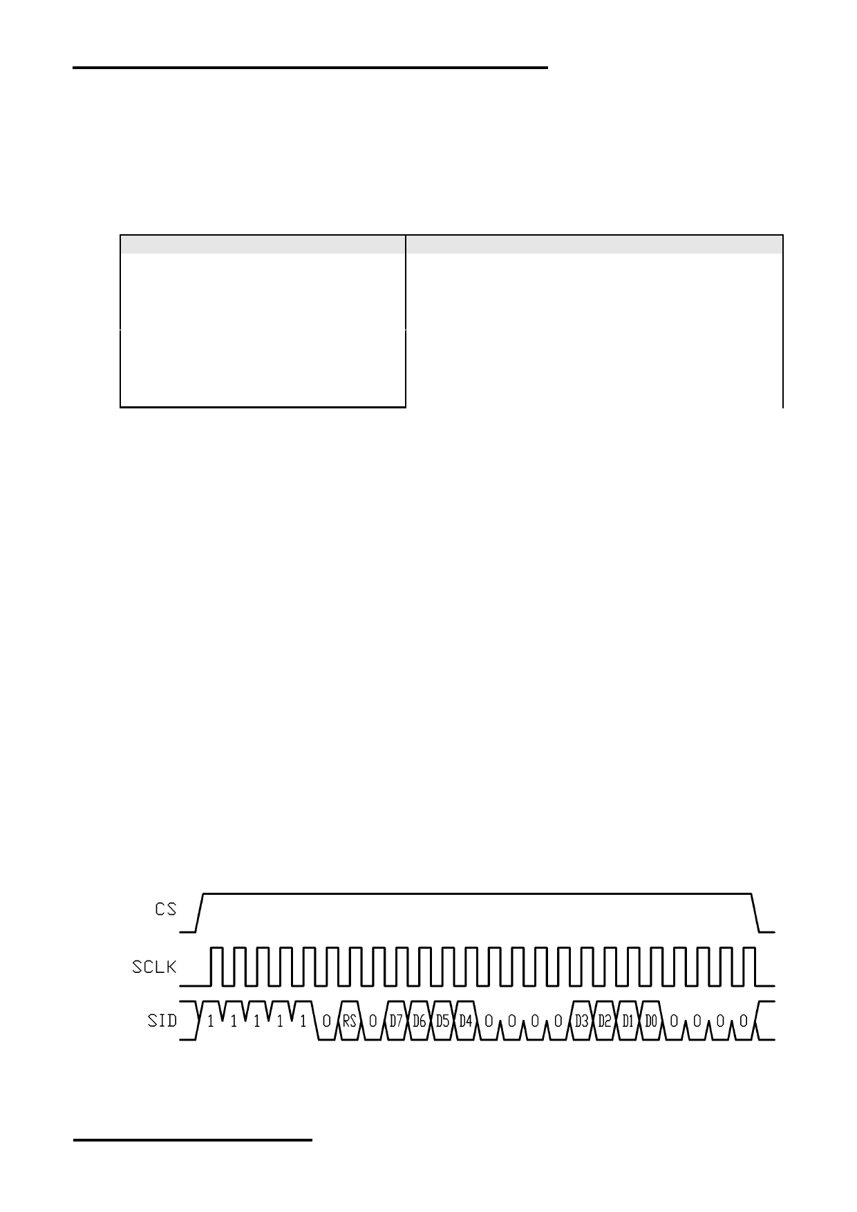
4.3 Using Serial interface
When PSB=L, the LCD module is in serial interface mode (write only).
In this mode, CS pin should be used. CS=H, enable the data transfer. CS=L, reset the serial
data counter, terminate the data transition and clear the data buffer.
As the controller IC have no instruction buffer area, it must wait for the previous instruction to
finish before sending the next one. Thus transferring multiple instruction/data, execution time
must be considered.
Starting a transmission, a start byte is required. It consists 5 consecutive “1” follow with a “0”,
a RS bit (Register Select bit) and a “0”.
Then the 8bit instruction/data should be separated into 2 groups. First group is DB7 to DB4,
followed by 4 consecutive “0”. The second group is DB3 to DB0 with 4 consecutive “0”.
See the Data Sequence Diagram for details.
Data Sequence Diagram (Serial Mode)
URL: www.topwaydisplay.com
Document Name: LM3033DDW-0B-Manual-Rev0.1
Page: 8 of 13
TOPWAY
LCD Module User Manual
LM3033DDW-0B
4.4 Display Memory Map
There are three main memory-areas in the LCD module for display.
- Character Generator RAM (CGRAM)
- Graphic Display RAM (GDRAM)
- Display Data RAM (DDRAM)
4.4.1 Character Generator RAM (CGRAM)
Character Generator RAM is for storing the User-defined Characters (a 16x16 dots font). There are
only four characters could be defined. The User-defined Character Codes are 0000h and 0002h.
They could be called into DDRAM as normal character.
User-defined
CGRAM
CGRAM data
Character Code
Address
D15 ~ D8
D7 ~ D0
00h
0000h
:
16 x 16 dot font
0Fh
10h
0002h
:
16 x 16 dot font
1Fh
20h
0004h
:
16 x 16 dot font
2Fh
30h
0006h
:
16 x 16 dot font
3Fh
CGRAM Address Map
4.4.2 Graphics Display RAM (GDRAM)
GDRAM is for full graphics display. It could be displayed when G=1 (set by EXTENDED
FUNCTION SET in Extended Instruction Set)
Horizontal Address (X)
00h
01h
~
06h
07h
D15 ~ D0
D15 ~ D0
~
D15 ~ D0
D15 ~ D0
00h
01h
:
:
:
1Eh
1Fh
00h
128x64 pixels
01h
:
:
:
1Eh
1Fh
D15 ~ D0
D15 ~ D0
~
D15 ~ D0
D15 ~ D0
08h
09h
~
0Eh
0Fh
Horizontal Address (X)
GDRAM Address Map
Note:
*1. The mapping is based on Vertical Scroll Displacement Address=0.
*2. Another 128x64 Graphics Display RAM space is not showed. They could be displayed by adjusting the Vertical Scroll
Displacement Address value.
URL: www.topwaydisplay.com
Document Name: LM3033DDW-0B-Manual-Rev0.1
Page: 9 of 13
TOPWAY
LCD Module User Manual
LM3033DDW-0B
4.4.3 Display Data RAM (DDRAM)
GB Character Code (16bit, A1A0h~F7FFh) could write into DDRAM for displaying the Simplified
Chinese Character (16x16 dots font). User Characters (16bit, 0000h or 0002h) defined by user that
stored in CGRAM could also be used. The display character should be on grid only.
DDRAM Address (Lower 4bit)
00h
01h
02h
03h
04h
05h
06h
07h
H
L
H
L
H
L
H
L
H
L
H
L
H
L
H
L
80h
90h
DDRAM
Address
8 x 4 Characters
(Upper 4bit)
80h
(16x16 dots font)
90h
H
L
H
L
H
L
H
L
H
L
H
L
H
L
H
L
08h
09h
0Ah
0Bh
0Ch
0Dh
0Eh
0Fh
DDRAM Address (Lower 4bit)
DDRAM Address Map with 16x16 dots font
Note:
*1. The mapping is based on Vertical Scroll Displacement Address=0.
*2. Another 8x4(Characters) Display Data RAM space is not showed. They could be displayed by adjusting the Vertical Scroll
Displacement Address value.
Standard ASCII code (8bit, 00h~7Fh) could write into DDRAM for displaying the Standard ASCII
Character (8x16 dots font). The display character should be on grid only, and two characters
should be written in each write operation.
DDRAM Address (Lower 4bit)
00h
01h
02h
03h
04h
05h
06h
07h
H
L
H
L
H
L
H
L
H
L
H
L
H
L
H
L
80h
90h
DDRAM
Address
16 x 4 Characters
(Upper 4bit)
80h
(8x16 dots font)
90h
H
L
H
L
H
L
H
L
H
L
H
L
H
L
H
L
08h
09h
0Ah
0Bh
0Ch
0Dh
0Eh
0Fh
DDRAM Address (Lower 4bit)
DDRAM Address Map with 8x16 dots font
Note:
*1. The mapping is based on Vertical Scroll Displacement Address=0.
*2. Another 16x4(Characters) Display Data RAM space is not showed. They could be displayed by adjusting the Vertical Scroll
Displacement Address value.
URL: www.topwaydisplay.com
Document Name: LM3033DDW-0B-Manual-Rev0.1
Page: 10 of 13
TOPWAY
LCD Module User Manual
LM3033DDW-0B
4.5 Display Control Instructions
4.5.1 Basic Instruction Set
RE=0, basic instruction set
Code
Instructions
Function
Fill DDRAM with “20h”, and set DDRAM address
CLEAR
0
0
0
0
0
0
0
0
0
1
counter (AC) to “00h”
Set DDRAM address counter (AC) to “00h” and put
HOME
0
0
0
0
0
0
0
0
1
X cursor to origin.
DDRAM content no changed.
Set cursor position and display shift when doing
write or read operation
ENTRY
0
0
0
0
0
0
0
1 I/D S
I/D=1, cursor move right AC increased by 1
MODE
I/D=0, cursor move left, AC decreased by 1
S=1, toggle the shift of the entire display
(based on I/D defined direction)
D=1, display ON
D=0, display OFF
DISPLAY
0
0
0
0
0
0
1
D C
B
C=1, cursor ON
ON/OFF
C=0, cursor OFF
B=1, blink ON
B=0, blink OFF
CURSOR
Cursor position and display shift control.
DISPLAY
0
0
0
0
0
1 S/C R/L X
X
DDRAM content no changed.
CONTROL
DL=1, 8bit interface
FUNCTION
0
0
0
0
1 DL X RE X
X
DL=0, 4bit interface
SET
RE=1, extended instruction
RE=0; basic instruction
SET CGRAM
Set CGRAM address to address counter (AC)
0
0
0
1 AC5 AC4 AC3 AC2 AC1 AC0 Make sure that in extended instruction SR=0 (scroll
ADDR
or RAM address selected)
SET DDRAM
0
0 AC7 AC6 AC5 AC4 AC3 AC2 AC1 AC0
Set DDRAM address to address counter (AC),
ADDR
where AC7 =1, AC6=0
READ BF &
0
1 BF AC6 AC5 AC4 AC3 AC2 AC1 AC0
Read busy flag (BF) for completion of the internal
ADDR
operation, also read out the value of AC
Write data to internal RAM
(DDRAM, CGRAM,GDRAM)
WRITE RAM 1 0 D7 D6 D5 D4 D3 D2 D1 D0
For 16bit data, write two byte consecutively,
high byte first, then low byte
Read data from internal RAM
READ RAM
1
1 D7 D6 D5 D4 D3 D2 D1 D0
(DDRAM, CGRAM,GDRAM)
Note:
*1. For the details of the Display Control Instructions, please refer to Sitronix ST7920 series datasheet.
*2. RE is the selection byte of basic and extended instruction set. Each time altering the value of RE, it will remain. Thus, it is not
necessary to set RE every time when using the same group of instruction set
URL: www.topwaydisplay.com
Document Name: LM3033DDW-0B-Manual-Rev0.1
Page: 11 of 13

TOPWAY
LCD Module User Manual
LM3033DDW-0B
4.5.2 Extended Instruction Set
RE=1, extended instruction set
Code
Instructions
Function
SCROLL or
SR=1, enable vertical scroll position
RAM ADDR
0
0
0
0
0
0
0
0
1 SR
SR=0, enable CGRAM address (basic instruction)
SELECT
Toggle 1 out of 4 line (in DDRAM) of the display to
REVERSE
0
0
0
0
0
0
0
1 R1 R0
be reversed (initial value is R1 ,R0 = 0, 0
DL=1, 8bit interface
EXTENDED
DL=0, 4bit interface
RE=1, extended instruction
FUNCTION
0
0
0
0
1 DL X RE G
0
RE=0; basic instruction
SET
G=1, graphics display ON
G=0, graphics display OFF
SET
Set the address of vertical scroll
SCROLL
0
0
0
1 AC5 AC4 AC3 AC2 AC1 AC0 Make sure extended instruction SR=1, enable
ADDR
vertical scroll position.
SET
0
0
1 AC6 AC5 AC4 AC3 AC2 AC1 AC0 Set the GDRAM address to address counter (AC)
Dual byte command should write consecutively
GRAPHICS
First byte set the Vertical address AC6~AC0
RAM ADDR
0
0
1
0
0
0 AC3 AC2 AC1 AC0
Second byte set the Horizontal address AC3~AC0
Note:
*1. For the details of the Display Control Instructions, please refer to Sitronix ST7920 series datasheet.
*2. RE is the selection byte of basic and extended instruction set. Each time altering the value of RE, it will remain. Thus, it is not
necessary to set RE every time when using the same group of instruction set
URL: www.topwaydisplay.com
Document Name: LM3033DDW-0B-Manual-Rev0.1
Page: 12 of 13

TOPWAY
LCD Module User Manual
LM3033DDW-0B
5. Design and Handling Precaution
Please refer to "LCD-Module-Design-Handling-Precaution.pdf".
URL: www.topwaydisplay.com
Document Name: LM3033DDW-0B-Manual-Rev0.1
Page: 13 of 13