
LM32019CFW-2
LCD Module User Manual
Prepared by:
Checked by:
Approved by:
Cai
Date:2008-11-25
Date:
Date:
Rev.
Descriptions
Release Date
0.1
Preliminary new release
2008-11-25
URL:
www.topwaydisplay.com
Document Name: LM32019CFW-2-Manual-Rev0.1.DOC
www.topwaysz.com
Page: 1 of 14

TOPWAY
LCD Module User Manual
LM32019CFW-2
Table of Content
1.
Basic Specifications................................................................................................................ 3
1.1
Display Specifications ............................................................................................................................................ 3
1.2
Mechanical Specifications...................................................................................................................................... 3
1.3
Block Diagram........................................................................................................................................................ 3
1.4
Terminal Functions................................................................................................................................................. 4
2.
Absolute Maximum Ratings.................................................................................................... 5
3.
Electrical Characteristics........................................................................................................ 5
3.1
DC Characteristics ................................................................................................................................................. 5
3.2
LED Backlight Circuit Characteristics..................................................................................................................... 5
3.3
AC Characteristics ................................................................................................................................................. 6
4.
Function Specifications .......................................................................................................... 7
4.1
Adjusting the Display Contrast ............................................................................................................................... 7
4.2
Display Pixel Map (4Gray Scale)............................................................................................................................ 7
4.3
Command Packet Format ...................................................................................................................................... 8
5.
Design and Handling Precaution ......................................................................................... 14
URL:
www.topwaydisplay.com
Document Name: LM32019CFW-2-Manual-Rev0.1.DOC
www.topwaysz.com
Page: 2 of 14
TOPWAY
LCD Module User Manual
LM32019CFW-2
1. Basic Specifications
1.1
Display Specifications
1) LCD Display Mode
: STN, Negative, Transmissive
2) Display Color
: Display Data = “11” : Light Gray (*1)
: Display Data = “00” : Dark Blue (*2)
3) Driving Method
: 1/240 duty, 1/16 bias
4) Backlight
: White LED backlight
Note:
*1. Color tone may slightly change by Temperature and Driving Condition.
*2. The Color is defined as the inactive / background color
1.2
Mechanical Specifications
1) Outline Dimension
: 159.0 x 107.8 x 11.0 MAX.
see attached Outline Drawing for details
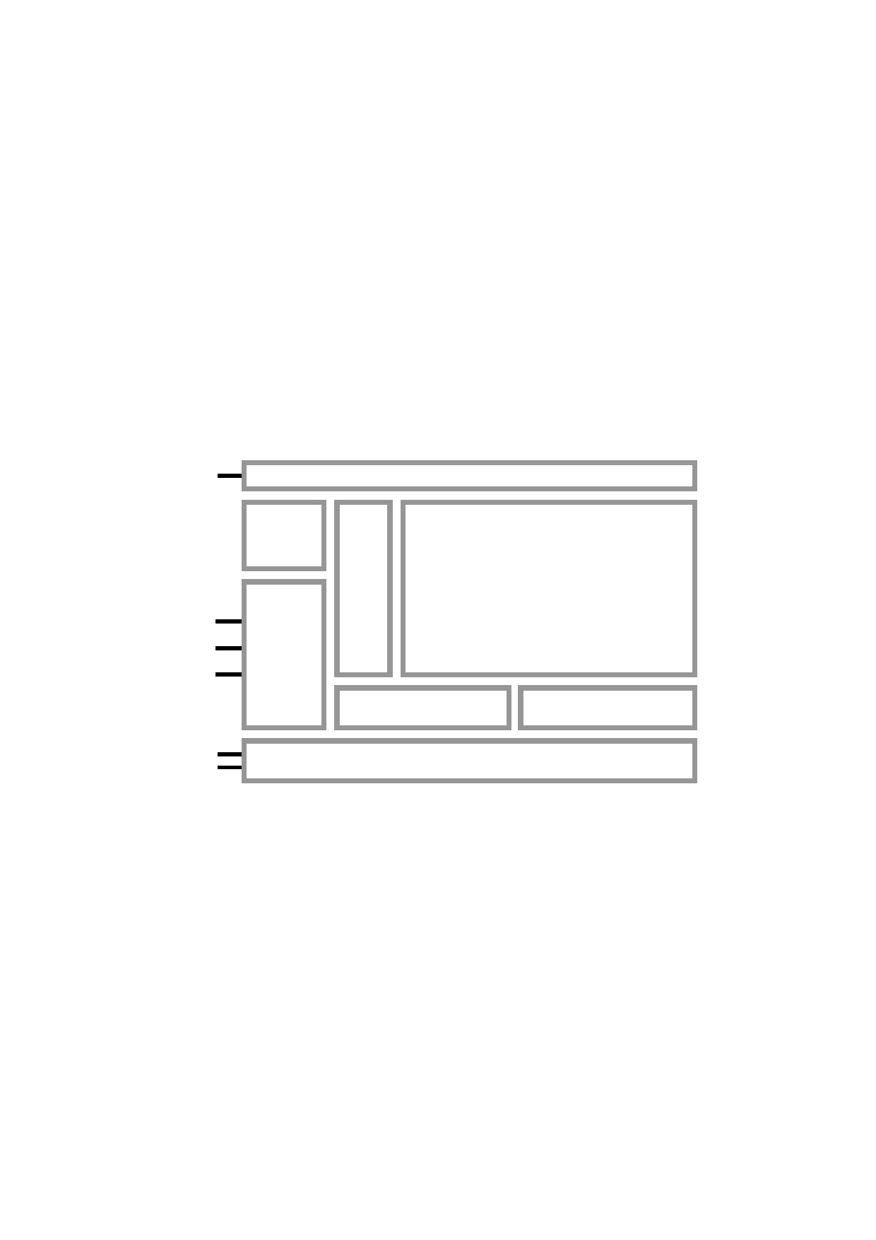
1.3
Block Diagram
BLA, BLK
Backlight Circuit
GB Char
ROM
320 x 240 pixels
LCD Panel
D0~D7
A1, /RD, /WR
/CS, /RESET, WAIT
SEG
SEG
Driver
Driver
VDD,VSS
VOUT, V0
Power Circuit
URL:
www.topwaydisplay.com
Document Name: LM32019CFW-2-Manual-Rev0.1.DOC
www.topwaysz.com
Page: 3 of 14

TOPWAY
LCD Module User Manual
LM32019CFW-2
1.4
Terminal Functions
Pin
Pin
No.
Name
I/O
Descriptions
1
VSS
Power
0V Power Supply, GND
2
VDD
Power
Positive Power Supply
3
V0
Input
LCD Contrast Reference Input
4
/WR
Input
Write enable input, active LOW
5
/RD
Input
Read enable input, active LOW
6
/CS
Input
Chip Select Inputs
/CS=LOW: Data IO is enabled
7
A1
Input
Register Select
A1=LOW:
Address[F004] is being accessed
Command Packet Port for Writing of Command Packets
A1=HIGH:
Address[F006] is being accessed
Port for writing Control or reading status
8
/RESET
Input
Reset Signal Input
/RESET=LOW: Reset
/RESET=HIGH: Normal
9
D0
I/O
8-bit bi-directional data bus
:
:
:
16
D7
I/O
17
/WAIT
Output
Wait signal
18
VOUT
Output
DC/DC power output for V0
19
BLA
Power
Positive Power Supply for LED backlight
20
BLK
Power
Negative Power Supply for LED backlight
URL:
www.topwaydisplay.com
Document Name: LM32019CFW-2-Manual-Rev0.1.DOC
www.topwaysz.com
Page: 4 of 14
TOPWAY
LCD Module User Manual
LM32019CFW-2
2. Absolute Maximum Ratings
Items
Symbol
Min.
Max.
Unit
Condition
Supply Voltage
V DD
-0.3
+5.5
V
V SS = 0V
Input Voltage
V IN
-0.3
+5.5
V
V SS = 0V
Operating Temperature
T OP
-20
70
° C
No Condensation
Storage Temperature
T ST
-30
80
° C
No Condensation
Cautions:
Any Stresses exceeding the Absolute Maximum Ratings may cause substantial damage to the device. Functional operation of this
device at other conditions beyond those listed in the specification is not implied and prolonged exposure to extreme conditions may
affect device reliability.
3. Electrical Characteristics
3.1
DC Characteristics
V SS =0V, V DD =5.0V, T OP =25 ° C
Items
Symbol
MIN.
TYP.
MAX.
Unit
Applicable Pin
Operating Voltage
V DD
4.8
5.0
5.2
V
VDD
Input High Voltage
V IH
3.0
-
VDD
V
Input pins, Bi-direction pins
Input Low Voltage
V IL
VSS
-
0.6
V
Input pins, Bi-direction pins
Output High Voltage
V OH
2.6
-
-
V
Bi-direction pins (*1)
Output Low Voltage
V OL
-
-
0.6
V
Bi-direction pins (*2)
LCD Contrast Reference
V0
Voltage
V 0
-
22.9
-
V
Operating Current(*3)
I DD
-
43.0
165
mA
VDD
Note:
*1. I OH =-3.0mA
*2. I OL = 3.0mA
3.2
LED Backlight Circuit Characteristics
BLK=0V, If BLA =153mA, T OP =25 ° C
Items
Symbol
MIN.
TYP.
MAX.
Unit
Applicable Pin
Forward Voltage
Vf BLA
-
5.0
-
V
BLA
Forward Current
If BLA
-
153
207
mA
BLA
Cautions:
Exceeding the recommended driving current could cause substantial damage to the backlight and shorten its lifetime.
BLA
BLK
No. of LED = 9pcs
URL:
www.topwaydisplay.com
Document Name: LM32019CFW-2-Manual-Rev0.1.DOC
www.topwaysz.com
Page: 5 of 14
TOPWAY
LCD Module User Manual
LM32019CFW-2
3.3
AC Characteristics
3.3.1 Write Timing
V SS =0V, V DD =5.0V, T OP =25 ° C
Symbol Parameter
Min
Max
Unit
t OHZ
Output Disable to Data Output in High-Z
0
15
ns
t AS
Address Setup Time
15
-
ns
t WP
Write Pulse Width
160
-
ns
t CW
Chip Select Assertion to Write Assertion
0
-
ns
t WC
Write Negation to Chip Select Negation
0
-
ns
t WR
Write Recovery Time
80
-
ns
t DS
Write Data to Write Assertion Setup
0
-
ns
Note:
T RISE and T FALL for all inputs must be ≤ 5 nsec (10% - 90%)
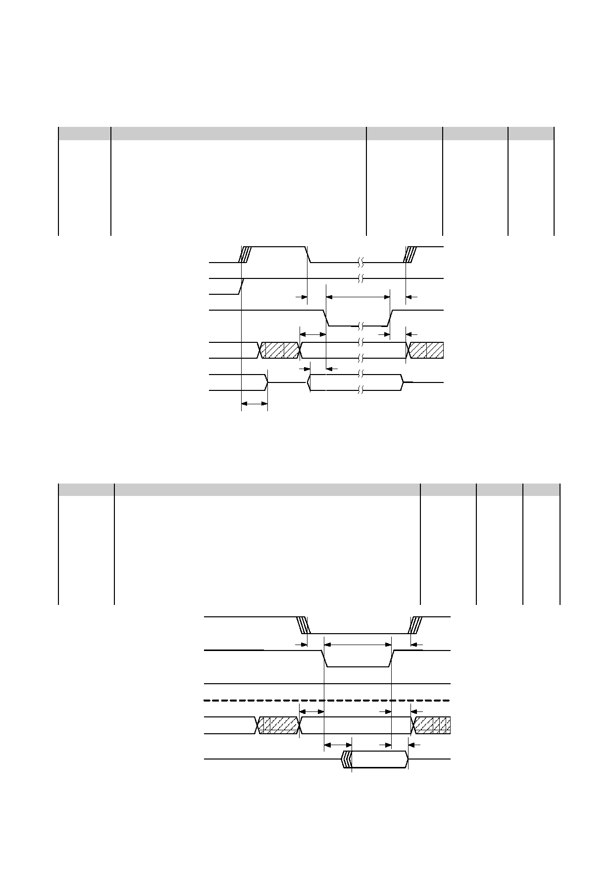
/CS
/RD
t CW
t WP
t WC
/WR
t AS
t WR
A1
t DS
D0~D7
VALID DATA
t OHZ
Host Interface - Write Timing Diagram
(for registers 0xF004 & 0xF006 only)
3.3.2 Read Timing
V SS =0V, V DD =5.0V, T OP =25 ° C
Symbol
Parameter
Min
Max
Unit
t CR
Chip Select Assertion to Read Assertion
0
-
ns
t RC
Read Negation to Chip Select Negation
0
-
ns
t AS
Address Setup Time
15
-
ns
t RP
Read Pulse Width
160
-
ns
t AH
Address Hold Time to Read Negation
80
-
ns
t OLZ
Read to Output in Low-Z
5
-
ns
t AC
Access Time
-
18
ns
t OHZ
Output Disable to Data Output in High-Z
0
13
ns
Note:
T RISE and T FALL for all inputs must be ≤ 5 nsec (10% - 90%)
/CS
t CR
t RP
t RC
/RD
/WR
t AS
t AH
A1
t AC
t OHZ
D0~D7
VALID DATA
Read Cycle asserted.
(for registers 0xF004 & 0xF006 only)
URL:
www.topwaydisplay.com
Document Name: LM32019CFW-2-Manual-Rev0.1.DOC
www.topwaysz.com
Page: 6 of 14
TOPWAY
LCD Module User Manual
LM32019CFW-2
4. Function Specifications
4.1
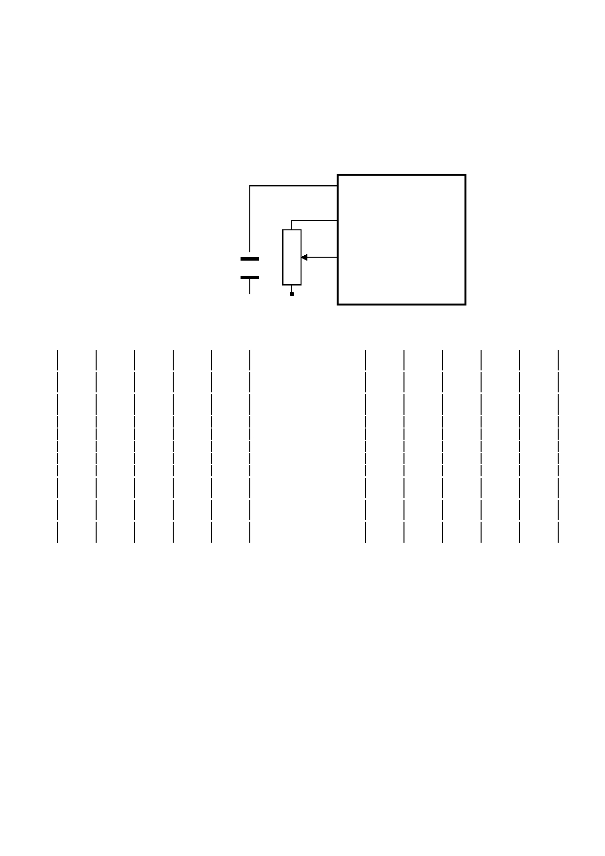
Adjusting the Display Contrast
A Variable-Resistor must be connected to the LCD module for providing a reference to V0.
Adjusting the VR will result the change of LCD display contrast.
The recommended value of VR is 25k to 50k
LCD module
VDD
VOUT
VR
V0
VSS
4.2
Display Pixel Map (4 Gray Scale)
1,1
2,1
3,1
4,1
5,1
316,1
317,1
318,1
319,1
320,1
(D7,D6)
(D5,D4)
(D3,D2)
(D1,D0)
(D7,D6)
- - -
- - -
(D1,D0)
(D7,D6)
(D5,D4)
(D3,D2)
(D1,D0)
1,2
2,2
3,2
4,2
5,2
316,2
317,2
318,2
319,2
320,2
(D7,D6)
(D5,D4)
(D3,D2)
(D1,D0)
(D7,D6)
- - -
- - -
(D1,D0)
(D7,D6)
(D5,D4)
(D3,D2)
(D1,D0)
1,3
2,3
3,3
4,3
5,3
316,3
317,3
318,3
319,3
320,3
(D7,D6)
(D5,D4)
(D3,D2)
(D1,D0)
(D7,D6)
- - -
- - -
(D1,D0)
(D7,D6)
(D5,D4)
(D3,D2)
(D1,D0)
:
:
:
:
:
:
:
:
:
:
:
:
:
:
:
:
:
:
:
:
:
:
:
:
:
:
:
:
:
:
:
:
:
:
:
:
1,238
2,238
3,238
4,238
5,238
316,238
317,238
318,238
319,238
320,238
(D7,D6)
(D5,D4)
(D3,D2)
(D1,D0)
(D7,D6)
- - -
- - -
(D1,D0)
(D7,D6)
(D5,D4)
(D3,D2)
(D1,D0)
1,239
2,239
3,239
4,239
5,239
316,239
317,239
318,239
319,239
320,239
(D7,D6)
(D5,D4)
(D3,D2)
(D1,D0)
(D7,D6)
- - -
- - -
(D1,D0)
(D7,D6)
(D5,D4)
(D3,D2)
(D1,D0)
1,240
2,240
3,240
4,240
5,240
316,240
317,240
318,240
319,240
320,240
(D7,D6)
(D5,D4)
(D3,D2)
(D1,D0)
(D7,D6)
- - -
- - -
(D1,D0)
(D7,D6)
(D5,D4)
(D3,D2)
(D1,D0)
Pixel mapping (Top View)
Note:
*1.
Based on the top view of the LCD module,
the 1, 1 (x, y) pixel is the upper-left pixel;
the 320, 240 (x, y) pixel is the lower-right pixel.
*2.
For the details of memory mapping please refer to T8000 datasheet.
*3.
For 4 Gray Scale (2bpp) mode, the data arrangement [D(i),D(i-1)] represent one pixel.
URL:
www.topwaydisplay.com
Document Name: LM32019CFW-2-Manual-Rev0.1.DOC
www.topwaysz.com
Page: 7 of 14

TOPWAY
LCD Module User Manual
LM32019CFW-2
4.3
Commands and Registers
4.3.1 Command Packet Format
All commands are organized in packet with a 1 byte “Opcode” followed by optional parameters /
data.
Steps
A1
/RD
/WR
Data
Descriptions
1
0
1
0
Opcode
Command Opcode
2
0
1
0
Parameter
Parameter / Data
:
:
:
:
:
:
:
:
:
:
:
:
:
1
1
0
01(hex)
Command End, Display On
-
For matching the FIFO size, the command packet should not larger than 64byte
(exclude, the Command End)
-
For multi-byte parameter/data, send LSB (low byte)first, MSB (highest byte) last.
4.3.2 Opcode Description
Opcode
(HEX)
Operations
Parameters / Data
00
Set “Control & Status The value of this data (one byte) will be directly written to the Control & Status
Port” of the
register.
Command Interpreter
10
charset_config
Character Set (1 byte):
00: Built in 8x8 ASCII
01: 8x8 CGRAM (Embedded RAM)
02: 8x16 CGRAM (Embedded RAM)
03: 16x16 CGRAM (Embedded RAM)
04: 16x16 GB2312-80 (External ROM)
12
set_print_coord
Character Print Coordinates (4 bytes)
- x (2 bytes)
- y (2 bytes)
For 4GS, x = (multiple of 2) – 1
For 16GS, x = (multiple of 4) – 1
14
set_font_fgcolor
Character Foreground Color (2 bytes)
(same as td_fgcolor, with opcode = (20 HEX))
For 4GS: 2bpp, (0x0000 ~ 0x0003)
For 16GS: 4bpp (0x0000 ~ 0x000F)
15
set_font_bgcolor
Character Background Color (2 bytes)
For 4GS: 2bpp, (0x0000 ~ 0x0003)
For 16GS: 4bpp (0x0000 ~ 0x000F)
URL:
www.topwaydisplay.com
Document Name: LM32019CFW-2-Manual-Rev0.1.DOC
www.topwaysz.com
Page: 8 of 14

TOPWAY
LCD Module User Manual
LM32019CFW-2
Opcode
(HEX)
Operations
Parameters / Data
16
show_char
Display Character (1 or 2 bytes)
17
show_string
Display String
- Character count (1 byte)
(0 ≤ character count ≤ 63)
- String ( ≤ 63 bytes)
20
td_fgcolor
Set Foreground Color (2 bytes)
For 4GS: 2bpp, (0x0000 ~ 0x0003)
For 16GS: 4bpp (0x0000 ~ 0x000F)
23
draw_pixel
Draw Pixel
- x (2 bytes)
- y (2 bytes)
24
draw_line
Draw Line
- x_start (2 bytes)
- y_start (2 bytes)
- x_end (2 bytes)
- y_end (2 bytes)
26
draw_rect
Draw Hollow Rectangle (Box)
- x_start (2 bytes)
- y_start (2 bytes)
- x_end (2 bytes)
- y_end (2 bytes)
27
fill_rect
Fill Rectangle (Box)
- x_start (2 bytes)
- y_start (2 bytes)
- x_end (2 bytes)
- y_end (2 bytes)
28
draw_circle
Draw Circle
- x_center (2 bytes)
- y_center (2 bytes)
- radius (1 byte)
29
fill_circle
Fill Circle
- x_center (2 bytes)
- y_center (2 bytes)
- radius (1 byte)
81
set_mem_ptr
Set memory pointer
- address (3 bytes)
82
read_reg
Read register
- address (2 bytes)
ONLY used in RS232 serial host mode
83
write_reg
Write register
- address (2 bytes)
- data (1 byte)
84
write_mem
Write memory
- count (1 byte)
- data (up to 63 bytes)
8F
mem_clk_en
Enable memory clock
“69 45 61 67 6C 65” (6 bytes in HEX)
URL:
www.topwaydisplay.com
Document Name: LM32019CFW-2-Manual-Rev0.1.DOC
www.topwaysz.com
Page: 9 of 14

TOPWAY
LCD Module User Manual
LM32019CFW-2
4.3.3 Registers Table
Register
Reset
(HEX)
R/W
Value
Descriptions
F000
Read
1000 0000
Chip ID Port Always read back 80 (HEX)
Write “DE FC 0B” (HEX) to enable memory clock, same as command with
Write
OPCODE “8F”.
F001
Read
0000 0000
Chip Revision Port
only
Always read back 00 (HEX) for iEM8000
F004
Write
-
Command Packet Port -
only
Writing of Command Packets.
F006
Port for writing control or reading status
Write
Don’t Care
Bit[7:4]: Reserved
Bit[3] = 1
Bit[3] : DISPLAY ON / OFF
0 : DISPLAY ON
1 : DISPLAY OFF
Don’t Care
Bit[2:1] : Reserved
Bit[0] = 0
Bit[0] : End of Command
Write “1” after each command packet
Read
Don’t Care
Bit[7:1] : Reserved
Bit[0] = 0
Bit[0] : FIFO full
Read “1” if Command FIFO is full.
Hosts must read this bit = “0” before writing to Command Packet Port.
F080
Read /
0000 0000
Bit[7:6] : External SRAM Select
Write
Bit[7:6] = 11: Required setting
- 64Kx16 external SRAM connected
Bit[5] : Horizontal TFT Pulse Polarity
0: Active low
1: Active high
Bit[4] : Vertical TFT Pulse Polarity
0: Active low
1: Active high
Bit[3] : STN Panel I/F Data Width
0: 4-bit single
1: 8-bit single
Bit[2] : Color Mode Select
0: Monochrome
1: Color
Bit[1:0] : Color Depth Select
If Monochrome (Bit[2] = 0)
00: 1 bit-per-pixel
01: 2 bit-per-pixel
10: 4 bit-per-pixel
11: Reserved
If Color (Bit[2] = 1)
00: 16 bit-per-pixel (TFT panel)
01: 12 bit-per-pixel (CSTN panel)
10: Reserved
11: Reserved
F081
Read /
000 0000
Bit[7] : Reserved
Write
Bit[6:0] : Panel Horizontal Character Count – 1,
Panel Horizontal Character Count[8:0] supports horizontal panel size up to
128 characters or 1024 pixels.
F082
Read /
0000 0000
Bit[7:0] : Panel Line Count - 1 bit[7:0]
Write
F083
Read /
0
Bit[7:1] : Reserved
Write
Bit[0] : Panel Line Count – 1 bit[8],
Panel Line Count[8:0] supports vertical panel size up to 512 lines.
F084
Read /
0000 0000
Bit[7:0] :
Write
Display Start Position X Coordinate – 1 bit[7:0]
F085
Read /
00
Bit[7:2] : Reserved
Write
Bit[1:0] :
Display Start Position X Coordinate – 1 bit[9:8]
URL:
www.topwaydisplay.com
Document Name: LM32019CFW-2-Manual-Rev0.1.DOC
www.topwaysz.com
Page: 10 of 14

TOPWAY
LCD Module User Manual
LM32019CFW-2
Register
Reset
(HEX)
R/W
Value
Descriptions
F086
Read /
0000 0000
Bit[7:0]
Write
Display Start Position Y Coordinate – 1 bit[7:0]
F087
Read /
00
Bit[7:2] : Reserved
Write
Bit[1:0] :
Display Start Position Y Coordinate – 1 bit[9:8]
Display Start Position (X,Y) is for panning of the view port on a virtual display.
F088
Read /
0000 0000
LCD_LUT1
Write
Bit[7:4] : for Gray level 3
Bit[3:0] : for Gray level 2
F089
Read /
0000 0000
LCD_LUT0
Write
Bit[7:4] : for Gray level 1
Bit[3:0] : for Gray level 0
F08A
Read /
000 0000
Bit[7] : Reserved
Write
Bit[6:0] : Virtual Display Character count – 1
It supports horizontal virtual size up to 128 characters or 1024 pixels.
F08B
Read /
00 0000
Bit[7:6] : Reserved
Write
Bit[5:0] : WF count for STN panels
000000: WF pin toggles every frame
000001: WF pin toggles every 2 LP pulses
000010: WF pin toggles every 3 LP pulses ………
…………………………………………………….
111111: WF pin toggles every 64 LP pulses
F08C
Read /
0000
Bit[7:4] : Reserved
Write
Bit[3:0] : Horizontal non-display period
0000: 2 characters (16 pixels)
0001: 3 characters (24 pixels) ………………….
…………………………………………………..
1111: 17 characters (136 pixels)
F08D
Read /
0000
Bit[7:4] : Reserved
Write
Bit[3:0] : Vertical non-display period
0000: 1 line
0001: 2 lines ……………………………………...
……………………………………………………
1111: 16 lines
F08E
Read /
0000 000
Bit[7:4] : Pixel Clock Divider
Write
0000: 24 MHz (divided by 1)
0001: 12 MHz (divided by 2)
0010: 8 MHz (divided by 3)
0011: 6MHz (divided by 4) ……………………
………………………………………………….
1111: 1.5MHz (divided by 16)
Bit[3] : Display Blank
0: Normal
1: Blank
Bit[2] : Display Invert
0: Normal
1: Invert
Bit[1] : LCD_ON Polarity
0: LCD_ON pin active low
1: LCD_ON pin active high
Bit[0] : Reserved
F08F
Read /
000 0000
Bit[7] : Reserved
Write
Bit[6:0] : Number of frames to start – 1
Maximum 128 frames
URL:
www.topwaydisplay.com
Document Name: LM32019CFW-2-Manual-Rev0.1.DOC
www.topwaysz.com
Page: 11 of 14

TOPWAY
LCD Module User Manual
LM32019CFW-2
Register
Reset
(HEX)
R/W
Value
Descriptions
F100
Read /
Bit[7:6]
Bit[7] – Enable / Disable
Write
= 00
0: Disable Sprite
1: Enable Sprite
Bit[6] – Transparency
0: Transparency disable
1: Transparency enable
When enabled: Sprite data = 00 becomes transparent and LCD background
will be displayed instead.
Bit[5:2] – Reserved
Bit[1:0]
Bit[1:0] – Sprite Modes Select
= 00
01: Sprite with 2 bit-per-pixel
00, 10, 11: Reserved
F102
Read /
0000 0000
Bit[7:0] - SP_LUT0L[7:0]
Write
F103
Read /
0000 0000
Bit[7:0] - SP_LUT0H[7:0]
Write
F104
Read /
0000 0000
Bit[7:0] - SP_LUT1L[7:0]
Write
F105
Read /
0000 0000
Bit[7:0] - SP_LUT1H[7:0]
Write
F106
Read /
0000 0000
Bit[7:0] - SP_LUT2L[7:0]
Write
F107
Read /
0000 0000
Bit[7:0] - SP_LUT2H[7:0]
Write
F108
Read /
0000 0000
Bit[7:0] - SP_LUT3L[7:0]
Write
F109
Read /
0000 0000
Bit[7:0] - SP_LUT3H[7:0]
Write
F10A
Read /
0000 0000
Bit[7:0] – Sprite Horizontal Pixel Count – 1
Write
Maximum 256 pixels
F10B
Read /
0000 0000
Bit[7:0] – Sprite Vertical Line Count – 1
Write
Maximum 256 lines
F10C
Read /
0000 0000
Bit[7:0] –
Write
Sprite Horizontal Start Position bit[7:0]
F10D
Read /
00
Bit[7:2] – Reserved
Write
Bit[1:0] - Sprite Horizontal Start Position bit[9:8]
Sprite Horizontal Start Position bit[9:0] is measured in pixels and counted from
left to right of the edge of the panel display (i.e. not virtual display).
F10E
Read /
0000 0000
Bit[7:0] –
Write
Sprite Vertical Start Position bit[7:0]
F10F
Read /
0
Bit[7:1] – Reserved
Write
Bit[0] - Sprite Vertical Start Position bit[8]
Sprite Vertical Start Position bit[8:0] is measured in lines and counted from top
to bottom of the edge of the panel display (i.e. not virtual display).
F142
Write
0000 0000
Bit[7:0] –
Only
Sprite / overlay storage starting address bit[7:0]
F143
Write
0000 0000
Bit[7:0] –
Only
Sprite / overlay storage starting address bit[15:8]
F144
Write
0000 0000
Bit[7:2] – Reserved
Only
Bit[1:0] –
Sprite / overlay storage starting address bit[17:16]
This is the starting address to put the sprite/overlay image
URL:
www.topwaydisplay.com
Document Name: LM32019CFW-2-Manual-Rev0.1.DOC
www.topwaysz.com
Page: 12 of 14

TOPWAY
LCD Module User Manual
LM32019CFW-2
Register
Reset
(HEX)
R/W
Value
Descriptions
F500
Read /
CS0 Configuration Port – Pulse Width
Write
Bit[7:4] =
Bit[7:4] : Write Cycle Pulse Width
1110
0000: 1 memory clock (24 MHz -> 41.6ns)
0001: 2 memory clocks
…………………………………………….
1110:15 memory clocks
Bit[3:0] =
1111: Reserved
1110
Bit[3:0] : Read Cycle Pulse Width
0000: 1 memory clock (24 MHz -> 41.6ns)
0001: 2 memory clocks
……………………………………………
1110:15 memory clocks
1111: Reserved
F501
Read /
0000 0000
CS0 Configuration Port – Control
Write
Bit[7] : Enable bit
0:Disable CS0
1:Enable CS0
Bit[6] : Memory data bus width
0: 8-bit memory data bus width
1: 16-bit memory data bus width
Bit[5] : 16-bit SRAM option
0:two 8-bit SRAMs
1:one 16-bit SRAM
Bit[4] : Reserved
Bit[3] : CS0 assertion time relative to address assertion.
0:CS0 and address assert at the same time
1:CS0 lags address by 1 memory clock.
Bit[2] : CS0 Negation Timing
0:CS0 and Address negate at the same time
1:CS0 leads Address by 1 memory clock in write access.
Bit[1] : Write Enable Assertion Time
0: Write Enable and Address Assert at the same time.
1: Write Enable lags Address by 1 memory clock.
Bit[0] : Write Enable Negation Time
0: Write Enable and Address negate at the same time.
1: Write Enable leads Address by 1 memory clock.
F504
Read /
CS1 Configuration Port – Pulse Width
Write
Bit[7:4] : Reserved
Bit[3:0] =
Bit[3:0] : Read Cycle Pulse Width
1110
0000: 1 memory clock (24 MHz -> 41.6ns)
0001: 2 memory clocks
0001: 3 memory clocks
………………………………………………
1101:14 memory clocks
1110:15 memory clocks
1111: Reserved
F505
Read /
0000 0000
CS1 Configuration Port – Control
Write
Bit[7] : Enable bit
0:Disable CS1
1:Enable CS1
Bit[6] : Memory data bus width
0: 8-bit memory data bus width
1: 16-bit memory data bus width
Bit[5] : Reserved
Bit[4] : Reserved
Bit[3] : CS1 assertion time relative to address assertion.
0:CS1 and Address assert at the same time
1:CS1 lags Address by 1 memory clock.
Bit[2] : CS1 Negation Timing
0:CS1 and Address negate at the same time
1:CS1 leads Address by 1 memory clock in write access.
Bit[1:0] : Reserved
F6C4
Read /
Bit[5:0] =
Set Memory Clock Divide
Write
11 0011
Bit[7:6] = Reserved
Bit[5:0] = 010000 to set 24MHz memory clock for proper operations
URL:
www.topwaydisplay.com
Document Name: LM32019CFW-2-Manual-Rev0.1.DOC
www.topwaysz.com
Page: 13 of 14

TOPWAY
LCD Module User Manual
LM32019CFW-2
5. Design and Handling Precaution
1.
The LCD panel is made by glass. Any mechanical shock (eg. dropping form high place)
will damage the LCD module.
2.
Do not add excessive force on the surface of the display, which may cause the Display
color change abnormally.
3.
The polarizer on the LCD is easily get scratched. If possible, do not remove the LCD
protective film until the last step of installation.
4.
Never attempt to disassemble or rework the LCD module.
5.
Only Clean the LCD with Isopropyl Alcohol or Ethyl Alcohol. Other solvents (eg. water)
may damage the LCD.
6.
When mounting the LCD module, make sure that it is free form twisting, warping and
distortion.
7.
Ensure to provide enough space (with cushion) between case and LCD panel to
prevent external force adding on it, or it may cause damage to the LCD or degrade the
display result.
8.
Only hold the LCD module by its side. Never hold LCD module by add force on the heat
seal or TAB.
9.
Never add force to component of the LCD module. It may cause invisible damage or
degrade of the reliability.
10.
LCD module could be easily damaged by static electricity. Be careful to maintain an
optimum anti-static work environment to protect the LCD module.
11.
When peeling off the protective film from LCD, static charge may cause abnormal
display pattern. It is normal and will resume to normal in a short while.
12.
Take care and prevent get hurt by the LCD panel sharp edge.
13.
Never operate the LCD module exceed the absolute maximum ratings.
14.
Keep the signal line as short as possible to prevent noisy signal applying to LCD
module.
15.
Never apply signal to the LCD module without power supply.
16.
IC chip (eg. TAB or COG) is sensitive to the light. Strong lighting environment could
possibly cause malfunction. Light sealing structure casing is recommend.
17.
LCD module reliability may be reduced by temperature shock.
18.
When storing the LCD module, avoid exposure to the direct sunlight, high humidity, high
temperature or low temperature. They may damage or degrade the LCD module
URL:
www.topwaydisplay.com
Document Name: LM32019CFW-2-Manual-Rev0.1.DOC
www.topwaysz.com
Page: 14 of 14