LMT035KDH03-NHN
LCD Module User Manual
Prepared by:
Checked by:
Approved by:
Liu sanyong
Date: 2018-03-19
Date:
Date:
Rev. Descriptions
Release Date
0.1
New release
2015-07-22
0.2
Add Terminal description and timing of SPI mode
2015-08-05
0.3
Update Section 2.1
2018-03-19
URL: www.topwaydisplay.com
Document Name: LMT035KDH03-NHN-Manual-Rev0.3
Page: 1 of 15

TOPWAY
LCD Module User Manual
LMT035KDH03-NHN
Table of Content
1. General Specification ............................................................................................................ 3
2. Block Diagram ........................................................................................................................ 3
2.1
Terminal Functions ............................................................................................................... 4
3. Absolute Maximum Ratings .................................................................................................. 4
4. Electrical Characteristics ...................................................................................................... 5
4.1
DC Characteristics ............................................................................................................... 5
4.2
AC Characteristics ................................................................................................................ 5
4.2.1
8080 Mode Timing ..................................................................................................... 5
4.2.2
SPI Mode Timing ....................................................................................................... 6
4.2.3
Reset Timing ............................................................................................................. 8
5. Optical Characteristics .......................................................................................................... 9
6. Function Specifications ....................................................................................................... 11
6.1
Command Summary .......................................................................................................... 11
7. Precautions of using LCD Modules .................................................................................... 13
Appendix A Inspection items and criteria for appearance defects ......................................... 14
URL: www.topwaydisplay.com
Document Name: LMT035KDH03-NHN-Manual-Rev0.3
Page: 2 of 15
TOPWAY
LCD Module User Manual
LMT035KDH03-NHN
1. General Specification
Screen Size(Diagonal) :
3.5 inch
Resolution :
320(RGB) x 240
Interface :
8bit MCU Interface
Color Depth :
16.7M color (24bit)
Dot Pitch :
0.219 x 0.219 (mm)
Pixel Configuration :
RGB Stripe
Display Mode :
Transmissive / Positive
Surface Treatment :
Anti-Glare Treatment
Viewing Direction :
12 o’clock
Outline Dimension :
92.7 x 72.0 x 9.75 (mm)
Active Area :
70.08 x 52.56 (mm)
Weight :
Approx 54g
Backlight :
LED, White
Operating Temperature :
-20 ~ +70°C
Storage Temperature :
-30 ~ +80°C
Note: Backlight color may slightly change over temperature and driving voltage.
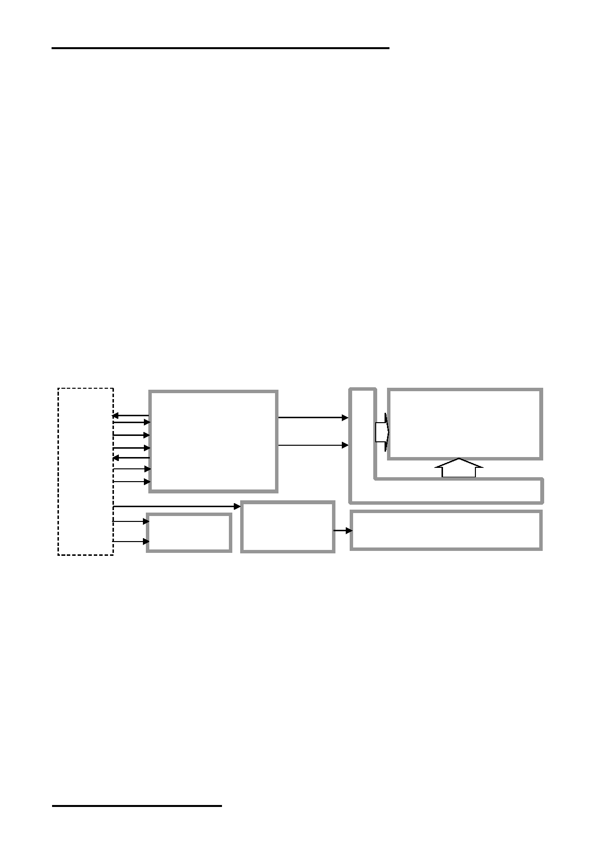
2. Block Diagram
K1
Driver Config
D0 ~ D7
Serial I/F
320(x3) x 240 pixels
A0
S1D13L01
Driver Display
TFT Panel
Signal
/RES, /CS
LCD Controller
TE
/WR, /RD
SPI_EN
TFT Driver
BL_ADJ
VDD
Power Circuit
Backlight Supply
Backlight Circuit
VSS
Figure 1
URL: www.topwaydisplay.com
Document Name: LMT035KDH03-NHN-Manual-Rev0.3
Page: 3 of 15
TOPWAY
LCD Module User Manual
LMT035KDH03-NHN
2.1 Terminal Functions
Terminal (K1)
Pin
Pin
8bit MCU Mode (Default)
SPI Mode
No.
Name
I/O
Description
Description
1
VSS
Power Input
Power Supply GND (0V)
2
3
VDD
Power Input
Positive Power Supply
4
Access Mode
5
A0
Input
A0=High: Accessing Data
Keep open
A0=Low: Accessing Address
6
/CS
Input
Chip Select
/CS=Low: Data IO is enabled
Reset
7
/RES
Input
/RES=Low: Reset
/RES=High: Normal operation
8
D0(SI)
Serial input
9
D1(SO)
Serial output
:
:
Bi-directional I/O
8-bit Bi-directional data bus
Keep open
14
D6
Keep open
15
D7
Keep open
16
TE
Output
TE Signal
17
/RD
Input
Read Enable, active Low
Keep open
18
/WR(SCK)
Input
Write Enable, active Low
Serial clock
19
BL_ADJ
Input
Backlight Driver enable signal, active High, PWM(*1) can be
possible
20
SPI_EN
Input
Keep open
SPI Enable, active high
21
22
NC
-
No connect
23
24
Note:
*1. The PWM frequency is between 200Hz and 500Hz.
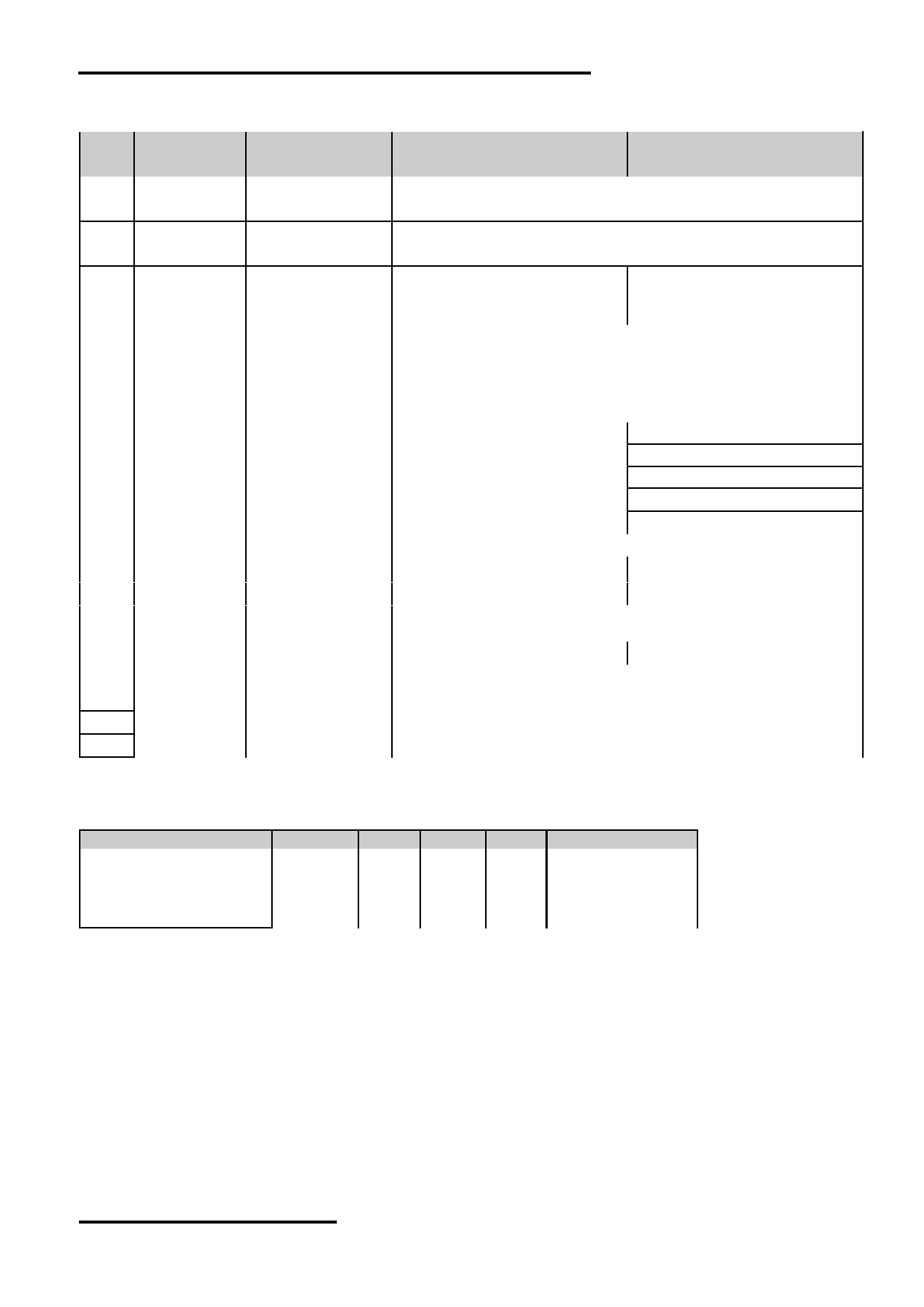
3. Absolute Maximum Ratings
Items
Symbol
Min.
Max.
Unit
Condition
Supply Voltage
V DD
-0.2
3.7
V
V SS = 0V
Input Voltage
V IN
-0.2
3.7
V
V SS = 0V
Operating Temperature
T OP
-20
+70
℃
No Condensation
Storage Temperature
T ST
-30
+80
℃
No Condensation
Caution:
Any Stresses exceeding the Absolute Maximum Ratings may cause substantial damage to the device. Functional
operation of this device at other conditions beyond those listed in the specification is not implied and prolonged exposure
to extreme conditions may affect device reliability.
URL: www.topwaydisplay.com
Document Name: LMT035KDH03-NHN-Manual-Rev0.3
Page: 4 of 15
TOPWAY
LCD Module User Manual
LMT035KDH03-NHN
4. Electrical Characteristics
4.1 DC Characteristics
V SS =0V, V DD =3.3V, T OP =25 ℃
Items
Symbol
MIN.
TYP.
MAX.
Unit
Applicable Pin
Operating Voltage
V DD
2.8
3.3
3.6
V
VDD
Input High Voltage
V IH
-
-
VDD
V
Input pins, Bi-direction pins
Input Low Voltage
V IL
VSS
-
-
V
Input pins, Bi-direction pins
Output High Voltage
V OH
2.6
-
-
V
Bi-direction pins (*1)
Output Low Voltage
V OL
-
-
0.6
V
Bi-direction pins (*2)
Operating Current
I DD
-
145
200
mA
On Backlight Power on status
4.2 AC Characteristics
4.2.1 8080 Mode Timing
A0
/CS Control
/CS
/WR
/RD
/RD,WR/ Control
/CS
/WR
/RD
Figure 2
3.3 Volt
Symbol
Parameter
Units
Min
Max
t1
A0 setup time to /CS (/WR, /RD)
1
-
ns
t2
/WR, /RD (/CS) setup time to /CS (/WR, /RD)
1
-
ns
t3
DB[7:0] setup time to /CS (/WR) rising edge: write cycle
1
-
ns
t4
DB[7:0] hold time from /CS (/WR) rising edge: write cycle
7
-
ns
t5w
/WR (/CS) hold time from /CS (/WR) rising edge: write cycle
3
-
ns
t5r
/RD (/CS) hold time from /CS (/RD) rising edge: read cycle
0
-
ns
t6
A0 hold time from /CS (/WR, /RD) rising edge
4
-
ns
t7
/CS (/RD) falling edge to DB[7:0] driven: read cycle
-
15
ns
t8
/CS (/RD) falling edge to valid Data: read cycle
-
4xT mclk +17
ns
t9
DB[7:0] hold time from /CS (/RD) rising edge: read cycle
2
12
ns
t10w
End of write to next read/write
5
-
ns
t10r
End of read to next read/write
T mclk +9
-
ns
t11w
/CS (/WR) pulse width for write cycle
3
-
ns
t12w
/CS (/WR) rise to next /CS (/WR) rise: write cycle
3xT mclk +6
-
ns
Note: T mclk = period of internal MCLK clock signal.
URL: www.topwaydisplay.com
Document Name: LMT035KDH03-NHN-Manual-Rev0.3
Page: 5 of 15
TOPWAY
LCD Module User Manual
LMT035KDH03-NHN
Indirect 8-bit Function Select:
A0
/WR
/RD
Comments
0
0
1
Command Write (register address)
1
0
1
Data (Parameter) Write
0
1
0
inhibit
1
1
1
Data (Parameter) Read
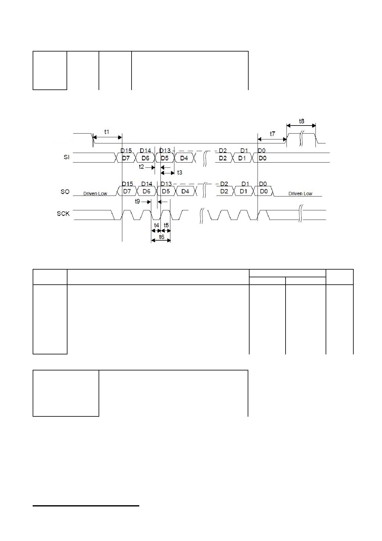
4.2.2 SPI Mode Timing
/CS
Figure 3
3.3 Volt
Symbol
Parameter
Units
Min
Max
t1
Chip select setup time
2
-
ns
t2
SI Data setup time
1
-
ns
t3
SI Data hold time
7
-
ns
t4
Serial clock pulse width low (high)
15
-
ns
t5
Serial clock pulse width high (low)
15
-
ns
t6
Serial clock period
30
-
ns
t7
Chip select hold time
7
-
ns
t8
Chip select de-assert to reassert
2
-
ns
t9
SCK falling edge to SO hold time
3
10
ns
SPI Function Select:
Command
Comments
10000000
8-bit Write
11000000
8-bit Read
10001000
16-bit Write
11001000
16-bit Read
the other
reserved
URL: www.topwaydisplay.com
Document Name: LMT035KDH03-NHN-Manual-Rev0.3
Page: 6 of 15
TOPWAY
LCD Module User Manual
LMT035KDH03-NHN
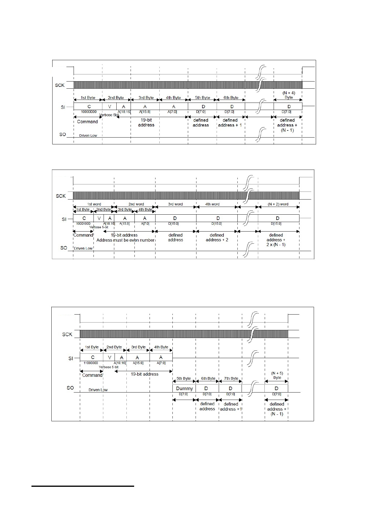
Write Procedure:
SPI 8bit Write Sequence:
/CS
Figure 4
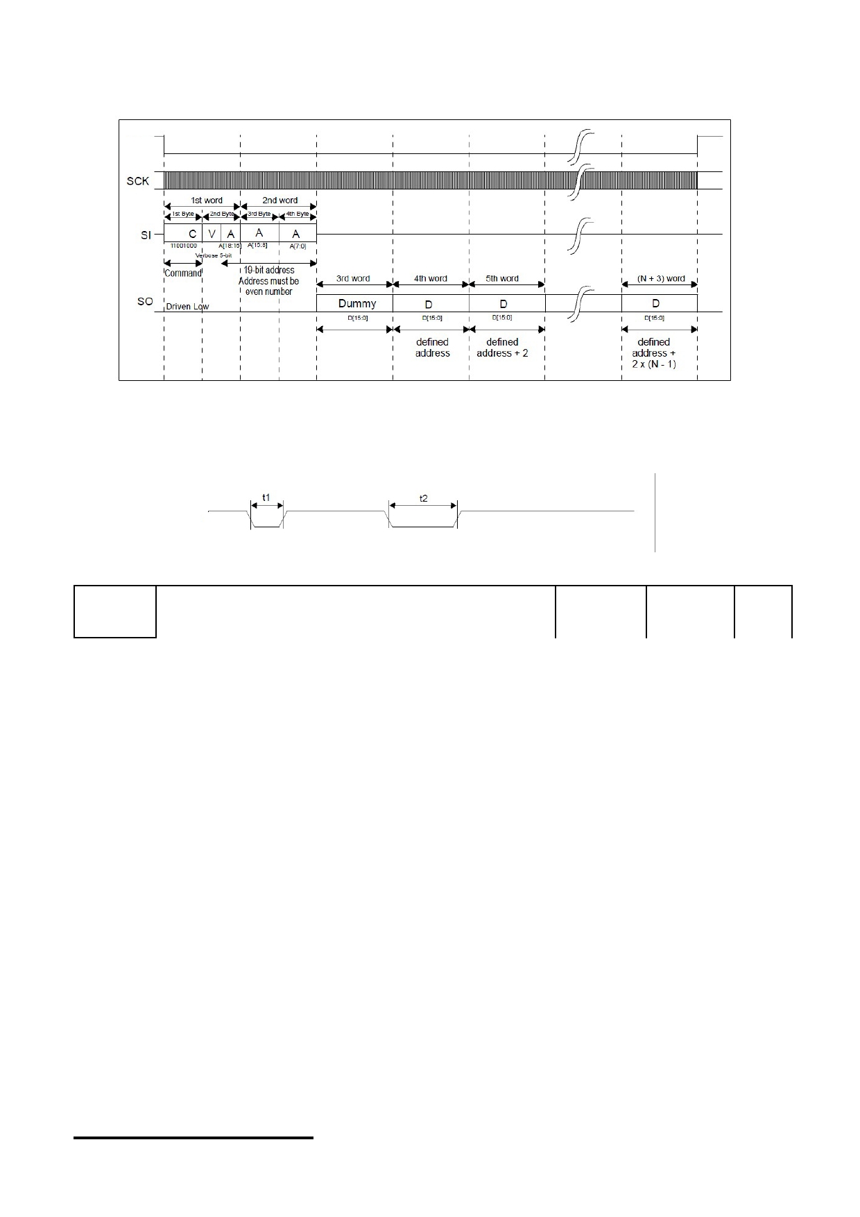
SPI 16bit Write Sequence:
/CS
Figure 5
Read Procedure:
SPI 8bit Read Sequence:
/CS
Figure 6
URL: www.topwaydisplay.com
Document Name: LMT035KDH03-NHN-Manual-Rev0.3
Page: 7 of 15
TOPWAY
LCD Module User Manual
LMT035KDH03-NHN
SPI 16bit Read Sequence:
/CS
Figure 7
4.2.3 Reset Timing
/RES
Figure 8
Symbol
Parameter
Min
Max
Units
t1
Reset Pulse Width is ignored
-
42
ns
t2
Active Reset Pulse Width (see Note)
150
-
ns
Note: The Reset input should be held low for longer than 150ns to guarantee reset.
For more information and details please refer to LCD controller (S1D13L01) datasheet.
URL: www.topwaydisplay.com
Document Name: LMT035KDH03-NHN-Manual-Rev0.3
Page: 8 of 15
TOPWAY
LCD Module User Manual
LMT035KDH03-NHN
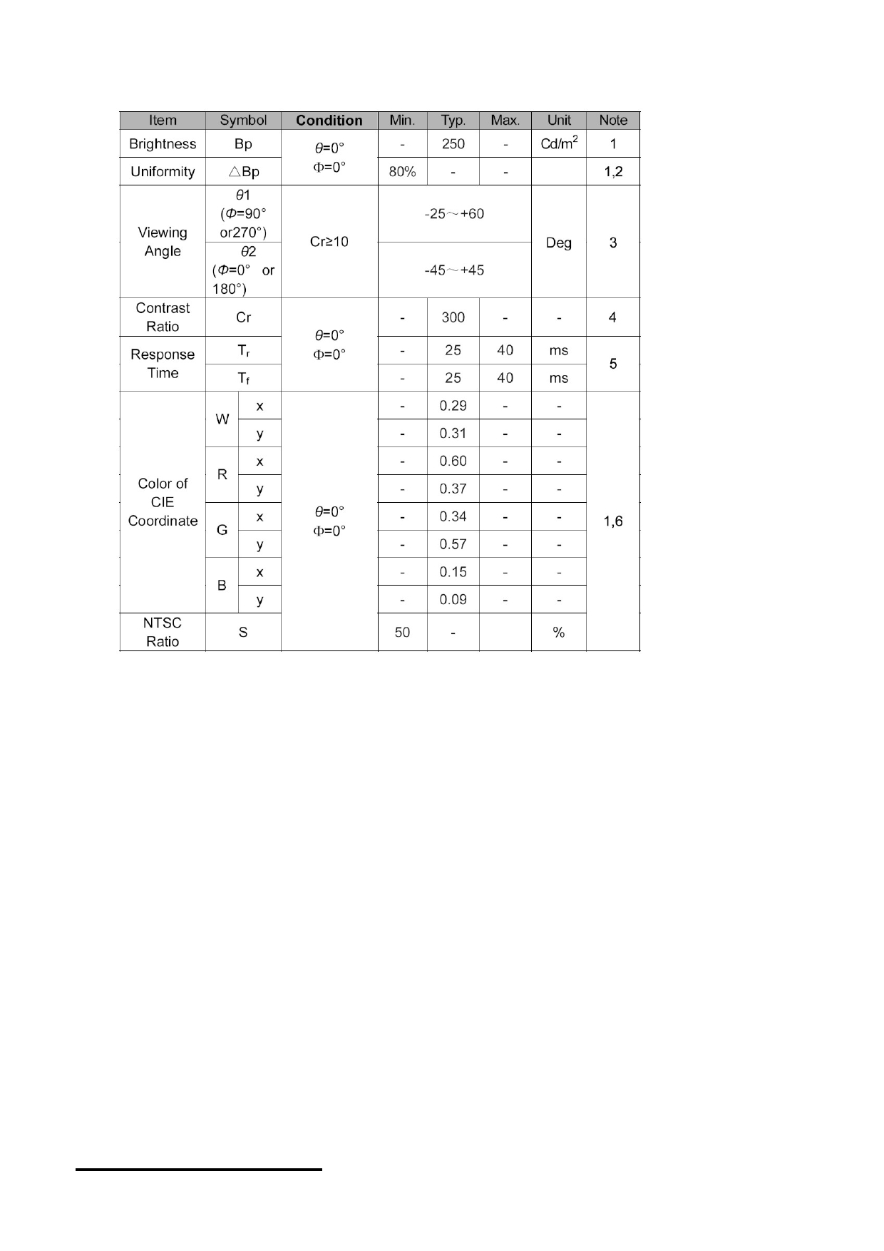
5. Optical Characteristics
Note : The parameter may slightly change over temperature, driving voltage and materials.
URL: www.topwaydisplay.com
Document Name: LMT035KDH03-NHN-Manual-Rev0.3
Page: 9 of 15
TOPWAY
LCD Module User Manual
LMT035KDH03-NHN
Note 1:
The data are measured after LEDs are turned on for 5
minutes. LCM displays full white. The brightness is the
average value of 9 measured spots. Measurement
equipment PR-705 (Φ8mm)
Measuring condition:
- Measuring surroundings: Dark room
- Measuring temperature: Ta=25 ℃ .
- Adjust operating voltage to get optimum
contrast at the center of the display.
Measured value at the center point of LCD panel after more
than 5 minutes while backlight turning on.
Note 2: reference Figure5
The luminance uniformity is calculated by using following
formula.
△ Bp = Bp (Min.) / Bp (Max.)×100 (%)
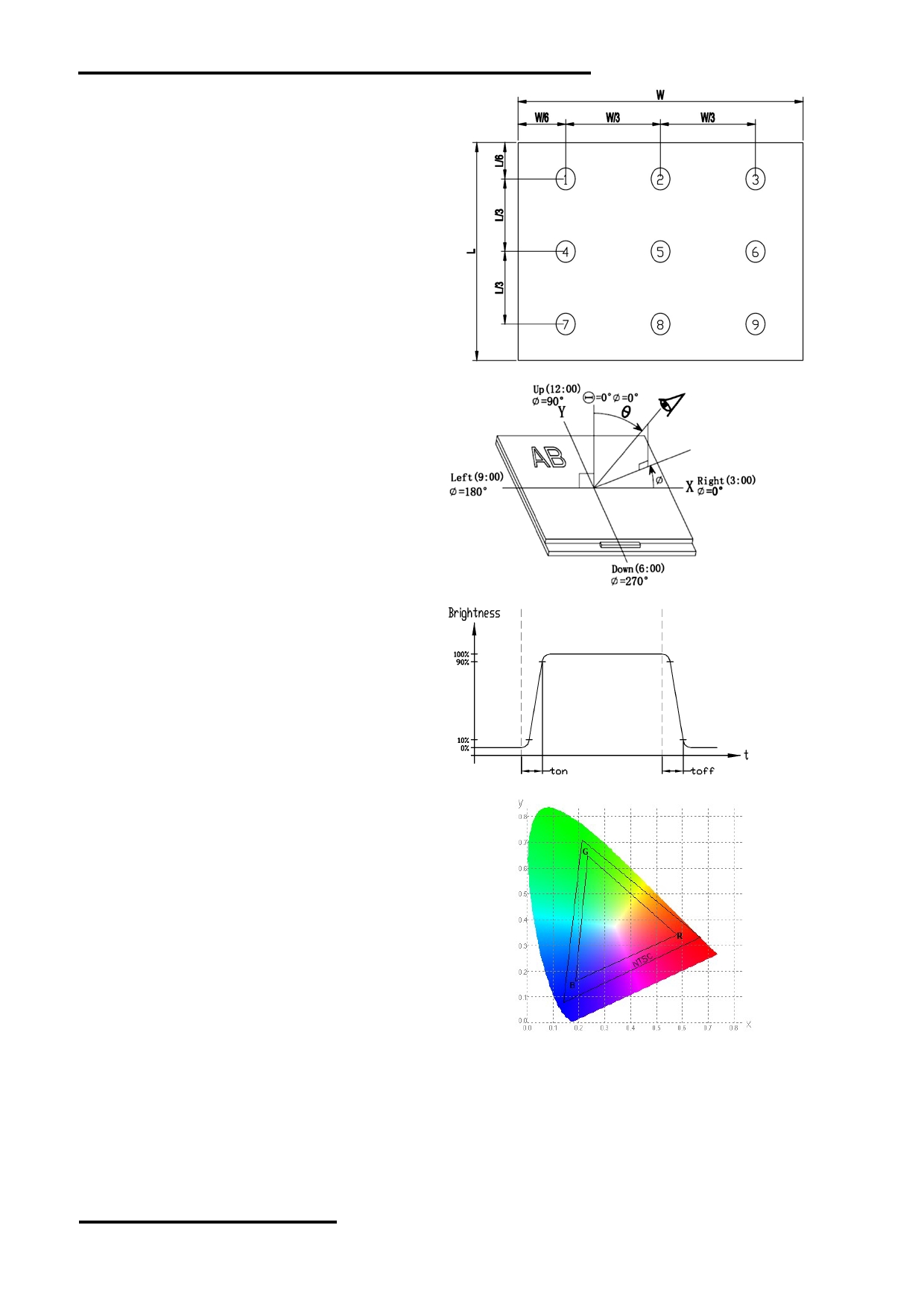
Bp (Max.) = Maximum brightness in 9 measured
Figure 9
spots
Bp (Min.) = Minimum brightness in 9 measured spots .
Note 3: reference Figure6
The definition of viewing angle:
Refer to the graph below marked by θ and Ф
Note 4:
The definition of contrast ratio (Test LCM using PR-705):
Figure 10
Contrast Luminance When LCD is at “White” state
Ratio(CR)= Luminance When LCD is at “Black” state
(Contrast Ratio is measured in optimum common electrode
voltage)
Note 5: reference Figure7
Definition of Response time. (Test LCD using DMS501):
The output signals of photo detector are measured
when the input signals are changed from
Figure 11
“black” to “white”(falling time)
and from “white” to “black”(rising time), respectively.
The response time is defined as
the time interval between the 10% and 90% of
amplitudes.Refer to figure as below.
Note 6: reference Figure8
Definition of Color of CIE Coordinate and NTSC Ratio.
Color gamut:
Area of RGB triangle
S=
X100%
Area of NTSC triangle
Figure 12
URL: www.topwaydisplay.com
Document Name: LMT035KDH03-NHN-Manual-Rev0.3
Page: 10 of 15
TOPWAY
LCD Module User Manual
LMT035KDH03-NHN
6. Function Specifications
6.1 Command Summary
Command
Para-
meter
HEX
Descriptions
Power Save
P1 60804 0 0 0
A[7:0]-> A[15:8] -> A[18:16]
Power Save Configuration Register
D[7:0]
1 0 0 n/a n/a n/a n/a n/a n/a Power Save Bit[1:0] = 00 , PSM0 mode
P2 D[15:8]
Bit[1:0] = 01 , PSM1 mode
1 0 0 n/a n/a n/a n/a n/a n/a n/a n/a
Bit[1:0] = 1x , NMM mode
Software
P1 60806 0 0 0
A[7:0]-> A[15:8] -> A[18:16]
Software Reset Register(Write Only)
Reset
D[7:0]
1 0 0 n/a n/a n/a n/a n/a n/a n/a n/a
D[15:8]
Softw Bit[8] = 0 , no effect in hardware
P2
1 0 0 n/a n/a n/a n/a n/a n/a n/a are Bit[8] = 1 , all registers are reset to default values
Reset
PLL Setting 0 P1 60810 0 0 0
A[7:0]-> A[15:8] -> A[18:16]
PLL Setting Register 0
D[7:0]
PLL PLL Bit[0] = 0 , the PLL is disabled
1 0 0 n/a n/a n/a n/a n/a n/a Bypa Enabl Bit[0] = 1 , the PLL enabled
Bit[1] = 0 , PLL is selected
P2
ss
e
D[15:8]
PLL
Bit[1] = 1 , CLKI is selected
1 0 0 Lock n/a n/a n/a n/a n/a n/a n/a Bit[15] = 0 , the PLL output is not stable
(RO)
Bit[15] = 1 , the PLL output is stable
PLL Setting 1 P1 60812 0 0 0
A[7:0]-> A[15:8] -> A[18:16]
PLL Setting Register 1
D[7:0]
1 0 0
M-Divider
Bit[9:0] 000h,001h … … 019h,020h : 1:1 ,2:1 … … 33:1(M-Divide Ratio).
P2 D[15:8]
021h to 13Fh: Reserved, PFDCLK = CLKI ÷ (M-Divider + 1)
1 0 0 n/a n/a
N-Counter
M-Divider
Bit[13:10] , must be set to 0000
PLL Setting 2 P1 60814 0 0 0
A[7:0]-> A[15:8] -> A[18:16]
PLL Setting Register 2
D[7:0]
1 0 0
L-Counter
Bit[9:0] , must be set between 010h ~ 041h. , and get the M-Divide Ratio
P2
D[15:8]
1 0 0 n/a n/a n/a n/a n/a n/a L-Counter from 17:1 to 66:1. POCLK = (L-Counter + 1) x (N-Counter + 1) x PFDCLK
Internal Clock P1 60816 0 0 0
A[7:0]-> A[15:8] -> A[18:16]
Internal Clock Configuration Register
Configuration
D[7:0]
P2
1 0 0 n/a n/a n/a n/a n/a PCLK Divide Select Bit[3:0] = 0000b,0001b … … 1110b,1111b : 1:1 ,2:1 … … 16:1(MCLK to
D[15:8]
1 0 0 n/a n/a n/a n/a n/a n/a n/a n/a PCLK Frequency Ratio)
Panel Setting P1 60820 0 0 0
A[7:0]-> A[15:8] -> A[18:16]
Panel Setting Miscellaneous Register
Miscellaneous
D[7:0]
Panel
Panel Bit[0] = 0 , TFT panel is disable
PCLK
Data Panel Data Port Bit[0] = 1 , TFT panel is enable
1 0 0 DE Polarity Polari n/a
Enabl
Width
Enabl Bit[2:1] = 01 , TFT 16-bit
ty
e
e
Bit[2:1] = 10 , TFT 18-bit
D[15:8]
Bit[2:1] = 11 , TFT 24-bit
Bit[3] = 0 , panel data is disable
P2
Bit[3] = 1 , panel data is enable
Bit[5] = 0, the LCD data outputs transition on the rising edge of PCLK
1 0 0 n/a n/a n/a n/a n/a n/a n/a n/a Bit[5] = 1 , the LCD data outputs transition on the falling edge of PCLK
Bit[7:6] = 00 , DE Polarity Low active
Bit[7:6] = 01 , DE Polarity High active
Bit[7:6] = 10 , DE Polarity Fixed to Low
Bit[7:6] = 11 , DE Polarity Fixed to High
Display
P1 60822 0 0 0
A[7:0]-> A[15:8] -> A[18:16]
Display Settings Register
Settings
D[7:0]
Displ
Panel Bit[0] = 0 , HS, VS, DE and PCLK are fixed to H or L and the display pipes
TE
Displ
ay
SW Interf are disabled
Statu
1 0 0
TE Function ay
n/a Blank Video ace Bit[0] = 1 , enable the panel output and display pipes
s
Blank
Polari Invert Enabl Bit[1] = 0 , video data is normal
(RO)
ty
es Bit[1] = 1 , video data is inverted
D[15:8]
Bit[2] = 0 , the display blank function operates normally
Bit[2] = 1 , the display blank function switches polarity
Bit[4] = 0 , the LCD data is masked
Bit[4] = 1 , all applicable LCD data outputs are forced to zero or one
P2
Bit[6:5] = 00b , TE output is disabled and the pin output is low
TE
Bit[6:5] = 01b , TE output is high (1) when the display is in the Vertical
Outp
Non-Display Period (VNDP) and low (0) when the display is in Vertical
1 0 0 n/a n/a n/a n/a n/a n/a n/a ut Pin
Display Period (VDISP)
Disab
Bit[6:5] = 10b , Line Count
le
Bit[6:5] = 11b , Reserved
Bit[7] = 0 , the selected condition in not occurring
Bit[7] = 1 , the selected condition in not occurring
Bit[8] = 0 , TE is output
Bit[8] = 1 , TE is not output
HDISP
P1 60824 0 0 0
A[7:0]-> A[15:8] -> A[18:16]
Horizontal Display Width Register (HDISP)
D[7:0]
Horizontal Display Width
P2
1 0 0 n/a
Bit[6:0] = horizontal display width in pixels ÷ 8
D[15:8]
1 0 0 n/a n/a n/a n/a n/a n/a n/a n/a
HNDP
P1 60826 0 0 0
A[7:0]-> A[15:8] -> A[18:16]
Horizontal Non-Display Period Register (HNDP)
D[7:0]
1 0 0 n/a
Horizontal Non-Display Period
P2
Bit[6:0] = horizontal non-display period in PCLK’s
D[15:8]
1 0 0 n/a n/a n/a n/a n/a n/a n/a n/a
VDISP
P1 60828 0 0 0
A[7:0]-> A[15:8] -> A[18:16]
Vertical Display Height Register (VDISP)
D[7:0]
1 0 0
Vertical Display Height
P2
D[15:8]
Vertical
Bit[9:0] = vertical display height in lines
1 0 0 n/a n/a n/a n/a n/a n/a
Display
Height
VNDP
P1 6082A 0 0 0
A[7:0]-> A[15:8] -> A[18:16]
Vertical Non-Display Period Register (VNDP)
D[7:0]
1 0 0
Vertical Non-Display Period
P2
Bit[7:0] = vertical non-display period in lines
D[15:8]
1 0 0 n/a n/a n/a n/a n/a n/a n/a n/a
URL: www.topwaydisplay.com
Document Name: LMT035KDH03-NHN-Manual-Rev0.3
Page: 11 of 15
TOPWAY
LCD Module User Manual
LMT035KDH03-NHN
Command
Para-
meter
HEX
Descriptions
HSW
P1 6082C 0 0 0
A[7:0]-> A[15:8] -> A[18:16]
HS Pulse Width Register (HSW)
D[7:0]
HS
Pulse
1 0 0
HS Pulse Width
Bit[6:0] = HS pulse width in PCLK’s
P2
Polari
Bit[7] = 0 , the horizontal sync signal is active low
ty
Bit[7] = 1 , the horizontal sync signal is active high
D[15:8]
1 0 0 n/a n/a n/a n/a n/a n/a n/a n/a
HPS
P1 6082E 0 0 0
A[7:0]-> A[15:8] -> A[18:16]
HS Pulse Start Position Register (HPS)
D[7:0]
HS Pulse Start Position
P2
1 0 0 n/a
Bit[6:0] = HS pulse start position in PCLK’s
D[15:8]
1 0 0 n/a n/a n/a n/a n/a n/a n/a n/a
VSW
P1 60830 0 0 0
A[7:0]-> A[15:8] -> A[18:16]
VS Pulse Width Register (VSW)
D[7:0]
VS
Pulse
1 0 0
n/a
VS Pulse Width
Bit[5:0] = VS pulse width in lines
P2
Polari
Bit[7] = 0 , the vertical sync signal is active low
ty
Bit[7] = 1 , the vertical sync signal is active high
D[15:8]
1 0 0 n/a n/a n/a n/a n/a n/a n/a n/a
VPS
P1 60832 0 0 0
A[7:0]-> A[15:8] -> A[18:16]
VS Pulse Start Position Register (VPS)
D[7:0]
VS Pulse Start Position
P2
1 0 0
Bit[7:0] = VS pulse start position in lines
D[15:8]
1 0 0 n/a n/a n/a n/a n/a n/a n/a n/a
TE Line Count P1 60834 0 0 0
A[7:0]-> A[15:8] -> A[18:16]
TE Line Count Register
D[7:0]
1 0 0
TE Line Count
These bits specify the line count value that is compared with the internal
P2 D[15:8]
TE Line
1 0 0 n/a n/a n/a n/a n/a n/a
vertical line counter
Count
Main Layer
P1 60840 0 0 0
A[7:0]-> A[15:8] -> A[18:16]
Main Layer Setting Register
Setting
D[7:0]
Main Layer
Main Layer Color
1 0 0 n/a n/a n/a
Rotation
Depth
Bit[2:0] = 000b, RGB 8:8:8 (default)
Select
Bit[2:0] = 001b, RGB 5:6:5
D[15:8]
Multi-
Bit[2:0] = 010b/011b/111b, Reserved
Byte
Bit[2:0] = 100b, 24 bpp + LUT1
Layer
Bit[2:0] = 101b, 16 bpp + LUT1
Regis
Bit[2:0] = 110b, 8 bpp + LUT1
P2
ters
Bit[4:3] = 00b, 0° (Normal)
Sync
1 0 0 n/a n/a n/a n/a n/a n/a n/a
Bit[4:3] = 01b, 90°
hrono
Bit[4:3] = 10b, 180°
us
Bit[4:3] = 11b, 270°
Latch
Bit[8] = 0, Synchronous latching of multi-byte layer registers is enabled
ing
Bit[8] = 1, Synchronous latching of multi-byte layer registers is disabled
Disab
le
Main Layer
P1 60842 0 0 0
A[7:0]-> A[15:8] -> A[18:16]
Main Layer Start Address Register 0
Start Address
D[7:0]
1 0 0
Main Layer Start Address
Bit[15:0] is Bit[15:0] of Main Layer Start Address ,but Bit[1:0] must be set
0
P2
D[15:8]
1 0 0
Main Layer Start Address
to 00b
Main Layer
P1 60844 0 0 0
A[7:0]-> A[15:8] -> A[18:16]
Main Layer Start Address Register 1
Start Address
D[7:0]
Main Layer Start
1 0 0 n/a
n/a
n/a
n/a
1
P2
Address
Bit[2:0] is Bit[18:16] of Main Layer Start Address
D[15:8]
1 0 0 n/a n/a n/a n/a n/a n/a n/a n/a
Main Layer
P1 60846 0 0 0
A[7:0]-> A[15:8] -> A[18:16]
Main Layer Width Register
Width
D[7:0]
1 0 0
Main Layer Width
P2 D[15:8]
Main Layer Read Only
1 0 0 n/a n/a n/a n/a n/a n/a
Width
Main Layer
P1 60848 0 0 0
A[7:0]-> A[15:8] -> A[18:16]
Main Layer Height Register
Height
D[7:0]
1 0 0
Main Layer Height
P2 D[15:8]
Main Layer Read Only
1 0 0 n/a n/a n/a n/a n/a n/a
Height
PIP Layer
P1 60850 0 0 0
A[7:0]-> A[15:8] -> A[18:16]
PIP Layer Setting Register
Setting
D[7:0]
1 0 0 n/a n/a n/a n/a n/a n/a n/a n/a Bit[2:0] = 000b, RGB 8:8:8 (default)
D[15:8]
Bit[2:0] = 001b, RGB 5:6:5
Bit[2:0] = 010b/011b/111b, Reserved
Bit[2:0] = 100b, 24 bpp + LUT1
PIP Layer
Bit[2:0] = 101b, 16 bpp + LUT1
P2
PIP Layer Color
1 0 0 n/a n/a n/a
Rotation
Bit[2:0] = 110b, 8 bpp + LUT1
Depth
Select
Bit[4:3] = 00b, 0° (Normal)
Bit[4:3] = 01b, 90°
Bit[4:3] = 10b, 180°
Bit[4:3] = 11b, 270°
PIP Layer
P1 60852 0 0 0
A[7:0]-> A[15:8] -> A[18:16]
PIP Layer Start Address Register 0
Start Address
D[7:0]
1 0 0
PIP Layer Start Address
Bit[15:0] is Bit[15:0] of Main Layer Start Address ,but Bit[1:0] must be set
0
P2
D[15:8]
1 0 0
PIP Layer Start Address
to 00b
PIP Layer
P1 60854 0 0 0
A[7:0]-> A[15:8] -> A[18:16]
PIP Layer Start Address Register 1
Start Address
D[7:0]
1 0 0 n/a n/a n/a n/a n/a n/a n/a n/a
1
P2 D[15:8]
PIP Layer Start
Bit[2:0] is Bit[18:16] of Main Layer Start Address
1 0 0 n/a n/a n/a n/a n/a
Address
PIP Layer
P1 60856 0 0 0
A[7:0]-> A[15:8] -> A[18:16]
PIP Layer Width Register
Width
D[7:0]
1 0 0
PIP Layer Width
Bit[9:] = PIP Layer Horizontal Display Period in number of pixels PIP
P2 D[15:8]
PIP Layer
1 0 0 n/a n/a n/a n/a n/a n/a
Layer Horizontal Display Period in number of pixels
Width
URL: www.topwaydisplay.com
Document Name: LMT035KDH03-NHN-Manual-Rev0.3
Page: 12 of 15
TOPWAY
LCD Module User Manual
LMT035KDH03-NHN
Command
Para-
meter
HEX
Descriptions
PIP Layer
P1 60858 0 0 0
A[7:0]-> A[15:8] -> A[18:16]
PIP Layer Height Register
Height
D[7:0]
1 0 0
PIP Layer Height
P2 D[15:8]
PIP Layer Bit[9:] = PIP Layer Vertical Display Period in number of lines
1 0 0 n/a n/a n/a n/a n/a n/a
Height
PIP Layer X
P1 6085A 0 0 0
A[7:0]-> A[15:8] -> A[18:16]
PIP Layer X Start Position Register
Start Position
D[7:0]
1 0 0
PIP Layer X Start Position
P2
D[15:8]
PIP Layer X
These bits specify X start position of the PIP Layer on the panel, in lines
1 0 0 n/a n/a n/a n/a n/a n/a
Start
Position
PIP Layer Y
P1 6085C 0 0 0
A[7:0]-> A[15:8] -> A[18:16]
PIP Layer Y Start Position Register
Start Position
D[7:0]
1 0 0
PIP Layer Y Start Position
P2
D[15:8]
PIP Layer Y
These bits specify Y start position of the PIP Layer on the panel, in lines
1 0 0 n/a n/a n/a n/a n/a n/a
Start
Position
PIP Enable
P1 60860 0 0 0
A[7:0]-> A[15:8] -> A[18:16]
PIP Enable Register
D[7:0]
Blink/
Bit[2:0] = 000b, Blank
Fade
Bit[2:0] = 001b, Normal
1 0 0 n/a n/a n/a n/a
Blink/Fade Effect
Status
Bit[2:0] = 010b, Blink 1
(RO)
Bit[2:0] = 011b, Blink 2
D[15:8]
Bit[2:0] = 100b, Fade Out
P2
Bit[2:0] = 101b, Fade In
Bit[2:0] = 110b, Fade In/Out Continuous
1 0 0
Blink/Fade Period
n/a Bit[2:0] = 111b, Reserved
Bit[3] = 0b, the PIP layer is not blinking or fading
Bit[3] = 1b, the PIP layer is in the process of blinking or fading
Bit[15:9] = blink/fade period in frames – 1
Alpha
P1 60862 0 0 0
A[7:0]-> A[15:8] -> A[18:16]
Alpha Blending Register
Blending
D[7:0]
1 0 0 n/a
Alpha Blending Ratio
Bit[6:0] = 0000000b,0000001b… …0111111b,1000000b :
D[15:8]
64:0 (no PIP),63:1 … … 1:63,0:64(full PIP) ;
1000001b ~ 1111111b : Reserved
P2
Alpha
Bit[9:8] = 00b, 1
1 0 0 n/a n/a n/a n/a n/a n/a
Blending
Bit[9:8] = 01b, 2
Step
Bit[9:8] = 10b, 4
Bit[9:8] = 11b, 8
Transparency P1 60864 0 0 0
A[7:0]-> A[15:8] -> A[18:16]
Transparency Register
D[7:0]
Transp
1 0 0 n/a n/a n/a n/a n/a n/a n/a arency Bit[0] = 0b, transparency is disabled
P2
Enable Bit[0] = 1b, transparency is enabled
D[15:8]
1 0 0 n/a n/a n/a n/a n/a n/a n/a n/a
Transparency P1 60866 0 0 0
A[7:0]-> A[15:8] -> A[18:16]
Transparency Key Color Register 0
Key Color 0
D[7:0]
Key Color Blue
Bit[15:8] is Key Color Green bits [7:0]
P2
1 0 0
D[15:8]
1 0 0
Key Color Green
Bit[7:0] is Key Color Blue bits [7:0]
Transparency P1 60868 0 0 0
A[7:0]-> A[15:8] -> A[18:16]
Transparency Key Color Register 1
Key Color 1
D[7:0]
Key Color Red
P2
1 0 0
Bit[7:0] is Key Color Red bits [7:0]
D[15:8]
1 0 0 n/a n/a n/a n/a n/a n/a n/a n/a
GPIO
P1 608D0 0 0 0
A[7:0]-> A[15:8] -> A[18:16]
GPIO Configuration Register
Configuration
D[7:0]
Bit[15:0] = 0b (default), the corresponding GPIO pin is configured as an
1 0 0 GPIO7 GPIO6 GPIO5 GPIO4 GPIO3 GPIO2 GPIO1 GPIO0
Config
Config
Config
Config
Config
Config
Config
Config input pin
P2
D[15:8]
Bit[15:0] = 1b , the corresponding GPIO pin is configured as an output pin
1 0 0 GPIO15 GPIO14 GPIO13 GPIO12 GPIO11 GPIO10 GPIO9 GPIO8
Config
Config
Config
Config
Config
Config
Config
Config
GPIO Status P1 608D2 0 0 0
A[7:0]-> A[15:8] -> A[18:16]
GPIO Status and Control Register
and Control
D[7:0]
1 0 0 GPIO7 GPIO6 GPIO5 GPIO4 GPIO3 GPIO2 GPIO1 GPIO0 When GPIOx is configured as an output:
Status
Status
Status
Status
Status Status
Status
Status
P2
Bit[15:0] = 0b, GPIOx low
D[15:8]
1 0 0 GPIO15 GPIO14 GPIO13 GPIO12 GPIO11 GPIO10 GPIO9 GPIO8 Bit[15:0] = 1b, GPIOx high
Status
Status
Status
Status
Status
Status
Status
Status
GPIO Pull-
P1 608D4 0 0 0
A[7:0]-> A[15:8] -> A[18:16]
GPIO Pull-Down Control Register
Down Control
D[7:0]
GPIO7
GPIO6
GPIO5
GPIO4
GPIO3
GPIO 2
GPIO1
GPIO0
1 0 0 Pull- Pull- Pull- Pull- Pull- Pull- Pull- Pull-
down
down
down
down
down
down
down
down
Bit[15:0] = 0b, the pull-down resistor for the associated GPIO pin is
Control
P2
Control
Control
Control
Control
Control
Control
Control
inactive.
D[15:8]
GPIO15 GPIO14 GPIO13 GPIO12 GPIO11 GPIO10 GPIO9
GPIO8
Bit[15:0] = 1b, the pull-down resistor for the associated GPIO pin is active.
1 0 0 Pull- Pull- Pull- Pull- Pull- Pull- Pull- Pull-
down
down
down
down
down
down
down
down
Control
Control
Control
Control
Control
Control
Control
Control
Note: Access of PLL Setting 0, PLL Setting 1, PLL Setting 2 and Internal Clock Configuration is only possible
in Power Save Mode PSM0.
For more information and details please refer to S1D13L01 datasheet.
7. Precautions of using LCD Modules
Please refer to "LCD-Module-Design-Handling-Precaution.pdf".
URL: www.topwaydisplay.com
Document Name: LMT035KDH03-NHN-Manual-Rev0.3
Page: 13 of 15
TOPWAY
LCD Module User Manual
LMT035KDH03-NHN
8. Appendix A Inspection items and criteria for appearance defects
Items
Criteria
Open Segment or Common
Not permitted
Short
Not permitted
Wrong Viewing Angle
Not permitted
Decliners
Not permitted
Contrast Ration Uneven
According to the limit specimen
Crosstalk
According to the limit specimen
White spots
X>1 pixel
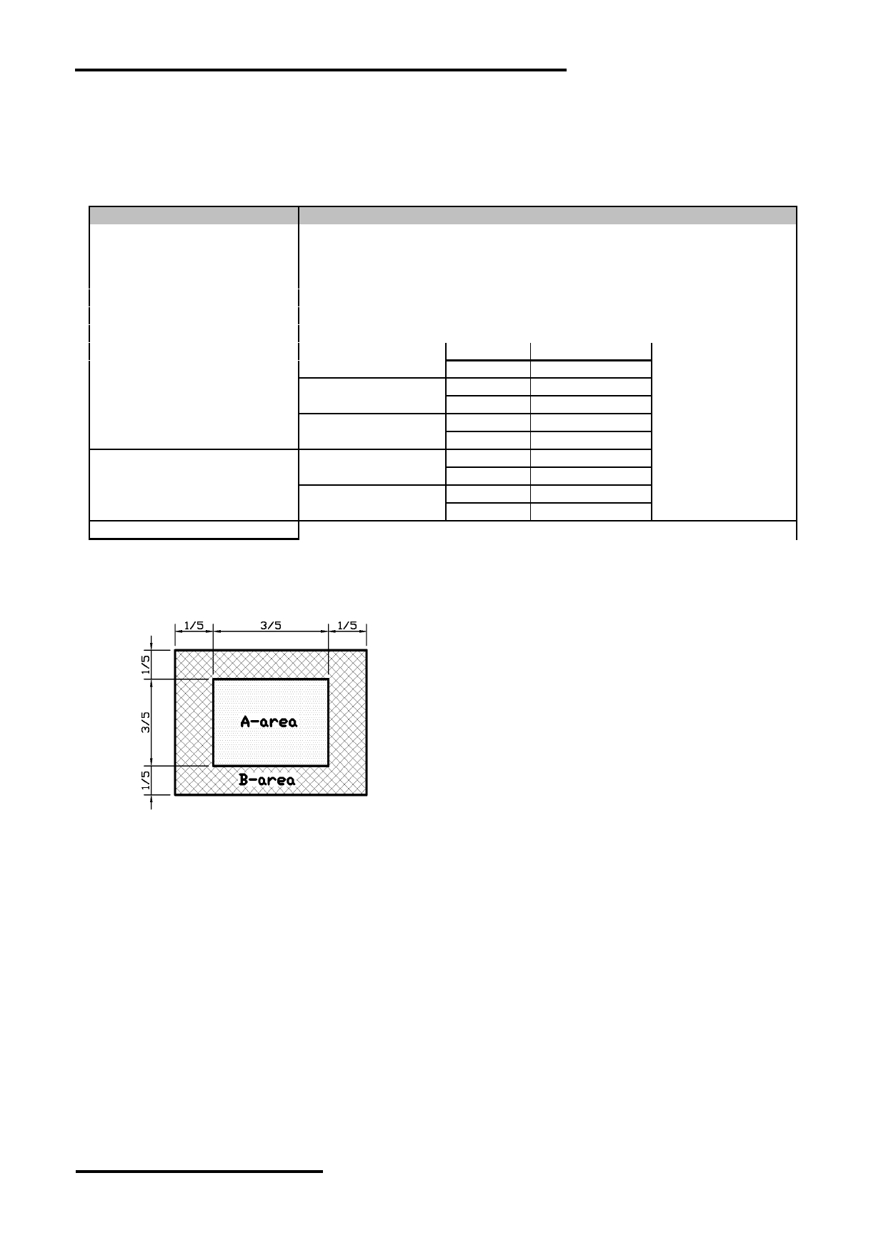
A-area
Not permitted
Max 6 spots
B-area
Max. 1 allowed
1/2 pixel<X≤1 pixel
A-area
Not permitted
allowed
B-area
Max. 2 allowed
X≤1/2 pixel
A-area
Max. 1 allowed
B-area
Max. 4 allowed
Black Sport
X>1 pixel
A-area
Not permitted
B-area
Max. 2 allowed
X≤1/2 pixel
A-area
Max. 1 allowed
B-area
Max. 4 allowed
Line Defect
Apparent vertical horizontal line defects are not permitted
Notes:
1. On Pixel includes 3 dots (RedDot + GreenDot + BlueDot)
2. Definition of Panel “A-area” and “B-area”
URL: www.topwaydisplay.com
Document Name: LMT035KDH03-NHN-Manual-Rev0.3
Page: 14 of 15