LMT035KDH03-NNA-1
LCD Module User Manual
Prepared by:
Checked by:
Approved by:
Lin Li
Date: 2018-10-18
Date:
Date:
Rev. Descriptions
Release Date
0.1
Preliminary
2012-03-22
0.2
Add T VS timing details and typical input data timing diagram in 5.3.1
2012-04-17
0.3
Update section 6
2018-10-18
URL: www.topwaydisplay.com
Document Name: LMT035KDH03-NNA-1-Rev0.3
Page: 1 of 22

TOPWAY
LCD Module User Manual
LMT035KDH03-NNA-1
Table of Content
1. General Specification ............................................................................................................ 3
2. Block Diagram ........................................................................................................................ 3
3. Terminal Functions ................................................................................................................ 4
3.1
Interface ............................................................................................................................... 4
4. Absolute Maximum Ratings .................................................................................................. 5
5. Electrical Characteristics ...................................................................................................... 5
5.1
DC Characteristics (MCU terminal)....................................................................................... 5
5.2
LED Backlight Circuit Characteristics ................................................................................... 5
5.3
AC Characteristics ................................................................................................................ 6
5.3.1
Display Data Input Timing .......................................................................................... 6
5.3.2
Active Display Timing................................................................................................. 8
5.3.3
Serial Command Interface (SPI) Timing ..................................................................... 9
6. Optical Characteristics ........................................................................................................ 10
7. Function Specifications ....................................................................................................... 12
7.1
SPI interface Data Packet .................................................................................................. 12
7.2
SPI interface Commands Summary.................................................................................... 13
7.3
SPI interface Commands Details ........................................................................................ 13
7.4
Power On/Off Sequence ..................................................................................................... 20
7.5
Standby Sequence ............................................................................................................. 21
7.6
Reset Function ................................................................................................................... 21
8. Precautions of using LCD Modules .................................................................................... 21
9. Appendix A <Inspection items and criteria for appearance defect> ................................ 22
URL: www.topwaydisplay.com
Document Name: LMT035KDH03-NNA-1-Rev0.3
Page: 2 of 22
TOPWAY
LCD Module User Manual
LMT035KDH03-NNA-1
1. General Specification
Screen Size(Diagonal) :
3.5 inch
Resolution :
320(RGB) x 240
Signal Interface :
24bit parallel bus / CCIR656 / 601
Color Depth :
16.7M color (24bit) *1
Dot Pitch :
0.219 x 0.219 (mm)
Pixel Configuration :
RGB Stripe
Display Mode :
Transmissive / Positive
Surface Treatment :
Anti-Glare Treatment
Viewing Direction :
12 o’clock
Outline Dimension :
76.9 x 63.9 x 4.25 (mm)
(exclude FPC, see attached drawing for details)
Active Area :
70.08 x 52.56 (mm)
Weight :
(TBD)
Backlight :
6 LEDs (in series)
Driver IC
NT39016D
Operating Temperature :
-20 ~ +70°C
Storage Temperature :
-30 ~ +80°C
Note:
*1 Color tune may slightly changed by temperature and driving voltage.
2. Block Diagram
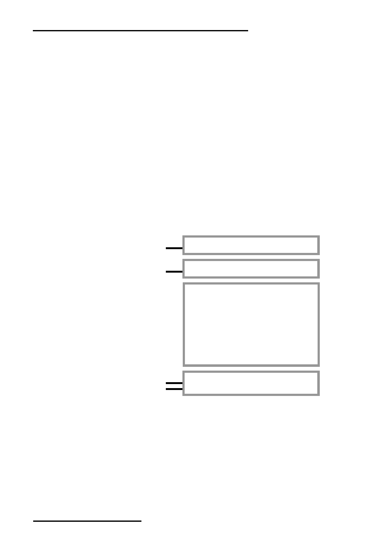
XR, YU, XL,YD
Touch Panel
LED_CATHODE, LED_ANODE
Backlight Circuit
320(x3) x 240 pixels
TFT Panel
D0~D23, HSYNC, VSYNC, DCLK, DEN
TFT Driver
VDD, GND
NT39016D or equivalent
/RST, /SPEN, SPCK, SPDA
URL: www.topwaydisplay.com
Document Name: LMT035KDH03-NNA-1-Rev0.3
Page: 3 of 22
TOPWAY
LCD Module User Manual
LMT035KDH03-NNA-1
3. Terminal Functions
3.1 TFT Interface
Pin Pin
No. Name
I/O
Descriptions
1
LED_CATHODE
P
Backlight LED Cathode supply
2
3
LED_ANODE
P
Backlight LED Anode supply
4
5
NC
-
No Connection
6
NC
-
7
NC
-
8
/RST
I
Reset signal active LOW
9
/SPEN
I
SPI enable signal, active LOW, normal HI (*1)
10
SPCK
I
SPI clock signal, rising edge trigger(*1)
11
SPDA
I/O
SPI data signal (*1)
12
D0
I
B0~B7,
:
:
Blue data input(*2)
19
D7
20
D8
I
G0~G7
:
:
Green data input (*2)
27
D15
28
D16
I
R0~R7(*2)
:
:
Read data input (*2)
35
D23
36
HSYNC
I
Horizontal Sync Signal
37
VSYNC
I
Vertical Sync Signal
38
DCLK
I
Data Clock Input
39
NC
--
No Connection
40
NC
--
41
VDD
P
Positive Power Supply
42
VDD
43
NC
--
No Connection
:
:
51
NC
52
DEN
I
Data Enable Input (*3)
53
GND
P
Power Ground Supply
54
GND
Note:
*1. /SPEN, SPCK, SPDA must be connected to referenced control pins to enable the SPI initialization
It may necessary to config the TFT Driver through SPI interface to provide best display result.
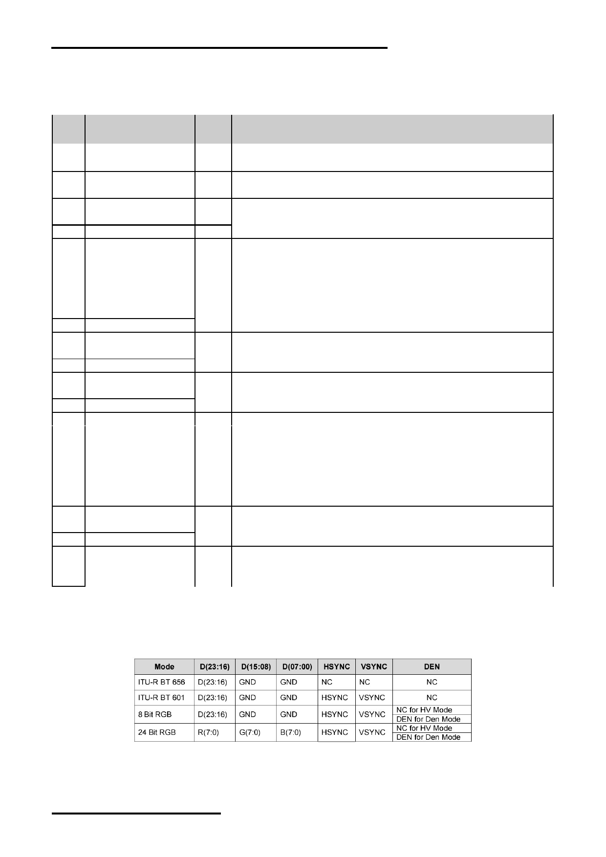
*2. For CCIR601/CCIR656 Interface, only R0-R7 is used. For unused pins (B0-B7,G0-G7), please
connect to GND or floating. The interface is selected by the SPI initial code.
Default setting is parallel 24-bit RGB interface.
*3: For digital RGB input data format, both SYNC mode and DE+SYNC mode are supported.
If DEN signal is fixed low. SYNC mode is used. Otherwise, DE+SYNC is used
URL: www.topwaydisplay.com
Document Name: LMT035KDH03-NNA-1-Rev0.3
Page: 4 of 22
TOPWAY
LCD Module User Manual
LMT035KDH03-NNA-1
4. Absolute Maximum Ratings
Items
Symbol
Min.
Max.
Unit
Condition
Supply Voltage
V DD
-0.3
+4.0
V
GND = 0V
Input Voltage
V IN
-0.3
+4.0
V
GND = 0V
Operating Temperature
T OP
-20
+70
C
No Condensation
Storage Temperature
T ST
-30
+80
C
No Condensation
Cautions:
Any Stresses exceeding the Absolute Maximum Ratings may cause substantial damage to the device. Functional operation of this
device at other conditions beyond those listed in the specification is not implied and prolonged exposure to extreme conditions may
affect device reliability.
5. Electrical Characteristics
5.1 DC Characteristics (MCU terminal)
GND=0V, V DD =3.3V, T OP =25 C
Items
Symbol
MIN.
TYP.
MAX.
Unit Applicable Pin
Operating Voltage
V DD
3.0
3.3
3.6
V
VDD
Input High Voltage
V IH
0.8VDD
-
VDD
V
Input pins
Input Low Voltage
V IL
GND
-
0.2VDD
V
Input pins
Frame Freq
F FRAME
-
60
-
Hz
Dot Data Clock(*1)
f DOTCLK
-
6.5
-
MHz
Operating Current(*2)
I DD
6.5
7.4
9.4
mA
VDD
Note.
*1. DOTCLK must be adapted to 19.5MHz in 8-bit mode
*2. test image is 16-grayscaly graphic
5.2 LED Backlight Circuit Characteristics
If LED_ANODE =20mA, T OP =25 C
Items
Symbol
MIN.
TYP.
MAX.
Unit Note
Forward Voltage
Vf LED_ANODE
-
19.2
-
V
Forward Current
If LED_ANODE
-
20
25
mA
Life Time
-
-
(50000)
-
hr
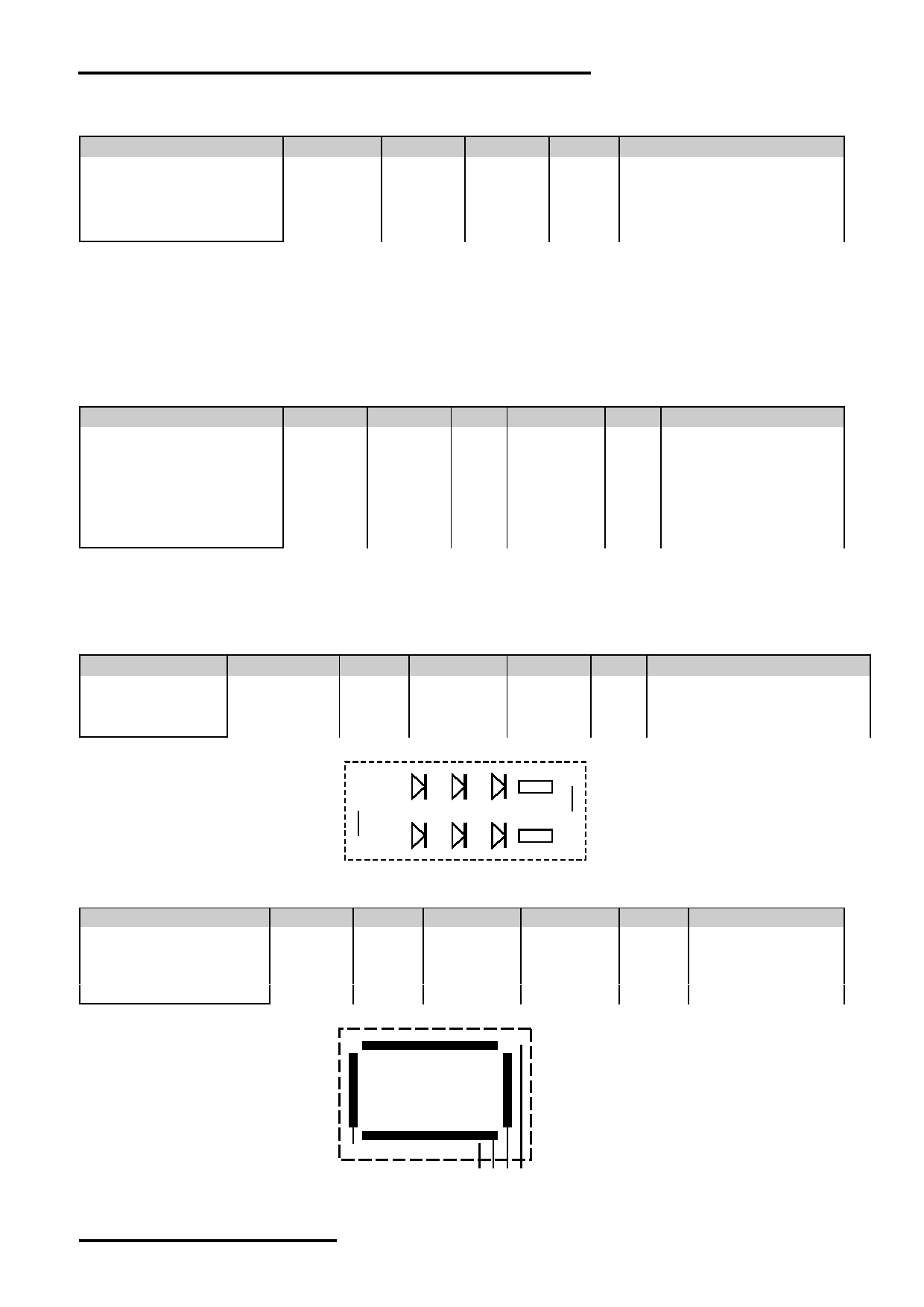
Cautions: Exceeding the recommended driving current could cause substantial damage to the backlight and shorten its lifetime.
LED_ANODE
LED_CATHODE
5.3 Touch panel Characteristics
No. of LEDs = 6 pcs
T OP =25 C
Items
Symbol
MIN.
TYP.
MAX.
Unit
Applicable Pin
Operating Voltage
V OP
-
5.0
-
V
XL, YD, XR, YU
Operating Force
Fop
60
-
100
g
-
Linearity
-
± 1.5
%
XL, YD, XR, YU
Life Time
-
-
1,000,000
-
times
-
Cautions: Exceeding the recommended Condition could cause substantial damage to the touch panel and shorten its lifetime.
URL: www.topwaydisplay.com
Document Name: LMT035KDH03-NNA-1-Rev0.3
Page: 5 of 22
TOPWAY
LCD Module User Manual
LMT035KDH03-NNA-1
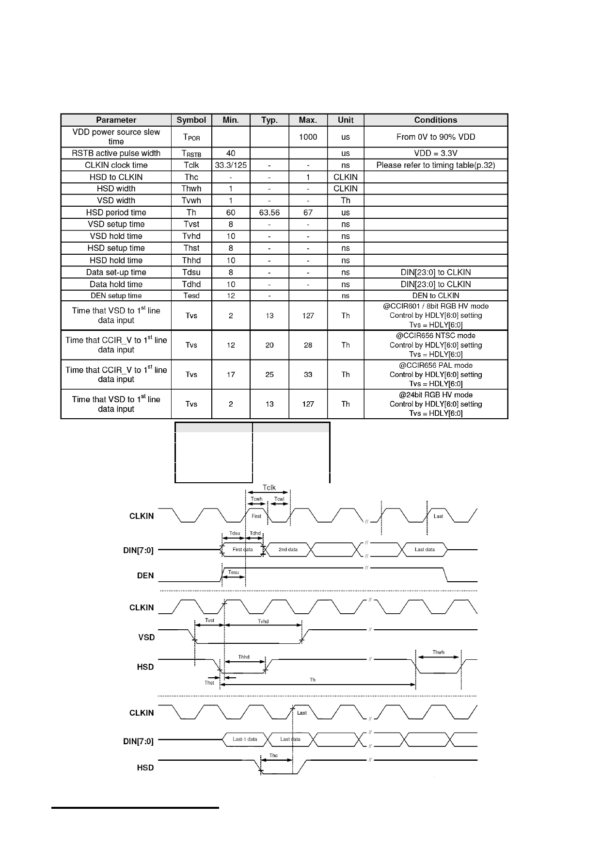
5.4 AC Characteristics
5.4.1 Display Data Input Timing
Signal naming references: Terminal Name
Signal Name
D23~D0
DIN[23:0]
DCLK
CLKIN
HSYNC
HSD
VSYNC
VSD
DEN
DEN
Timing Diagram
URL: www.topwaydisplay.com
Document Name: LMT035KDH03-NNA-1-Rev0.3
Page: 6 of 22

TOPWAY
LCD Module User Manual
LMT035KDH03-NNA-1
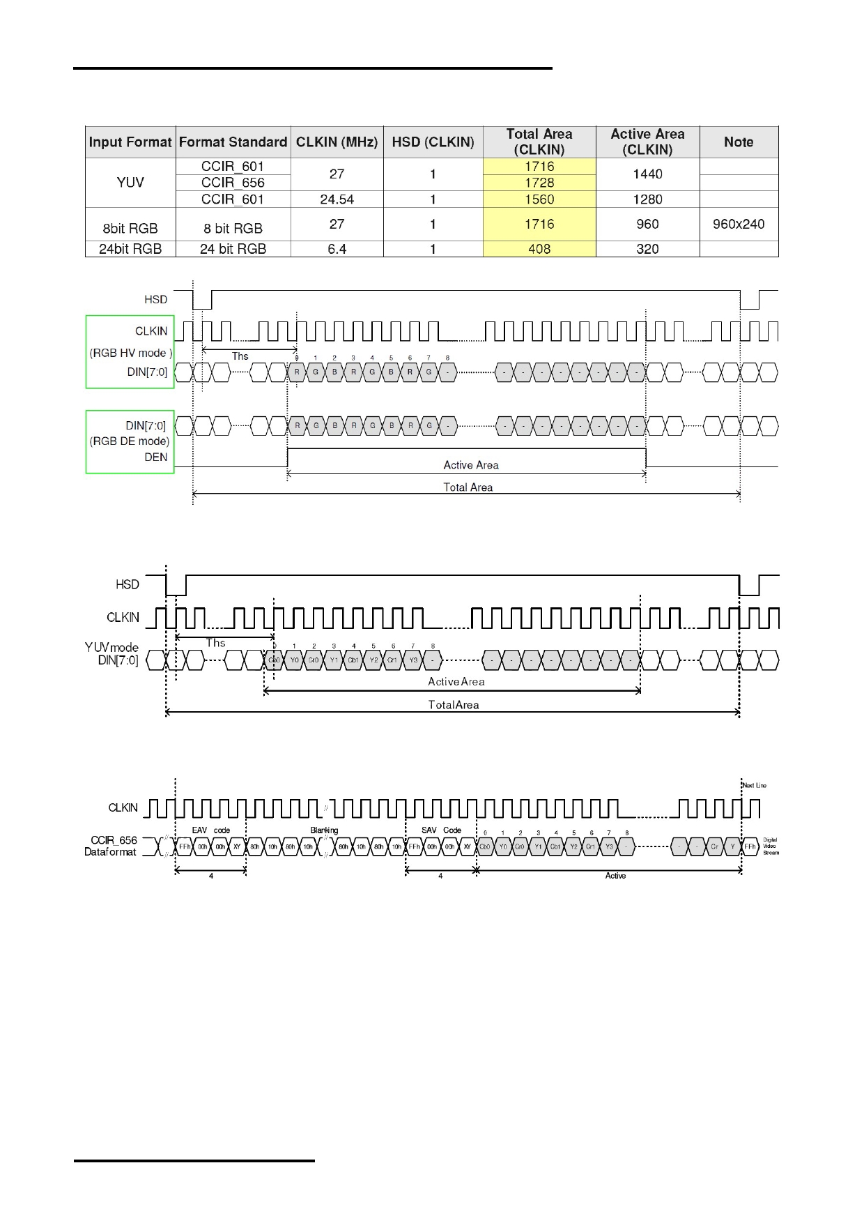
CCIR601 mode A/B
CCIR656 mode A/B
8bit RGB 960 CH Mode
24bit RGB mode (SEL[3:0]=1100 or 1101)
Typical Input Data Timing Diagram (24bit RGB mode SEL[3:0]=1100)
URL: www.topwaydisplay.com
Document Name: LMT035KDH03-NNA-1-Rev0.3
Page: 7 of 22
TOPWAY
LCD Module User Manual
LMT035KDH03-NNA-1
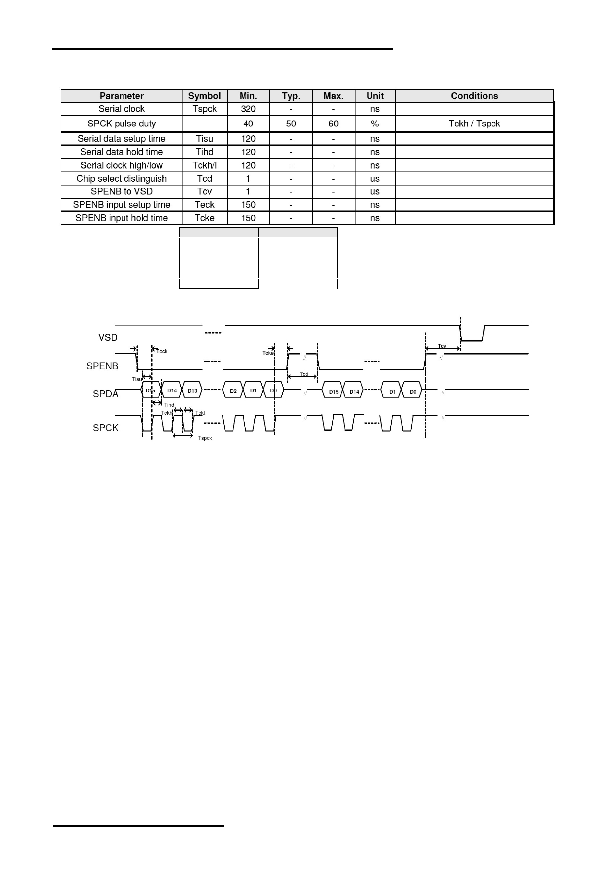
5.4.2 Active Display Timing
RGB input Data Format
YUV input Data Format
CCIR_656 input Data Format
URL: www.topwaydisplay.com
Document Name: LMT035KDH03-NNA-1-Rev0.3
Page: 8 of 22
TOPWAY
LCD Module User Manual
LMT035KDH03-NNA-1
5.4.3 SPI Interface Timing
Signal naming references: Terminal Name
Signal Name
SPDA
SPDA
SPCK
SPCK
VSYNC
VSD
/PSEN
PSENB
/RST
RSTB
Timing Diagram
URL: www.topwaydisplay.com
Document Name: LMT035KDH03-NNA-1-Rev0.3
Page: 9 of 22

TOPWAY
LCD Module User Manual
LMT035KDH03-NNA-1
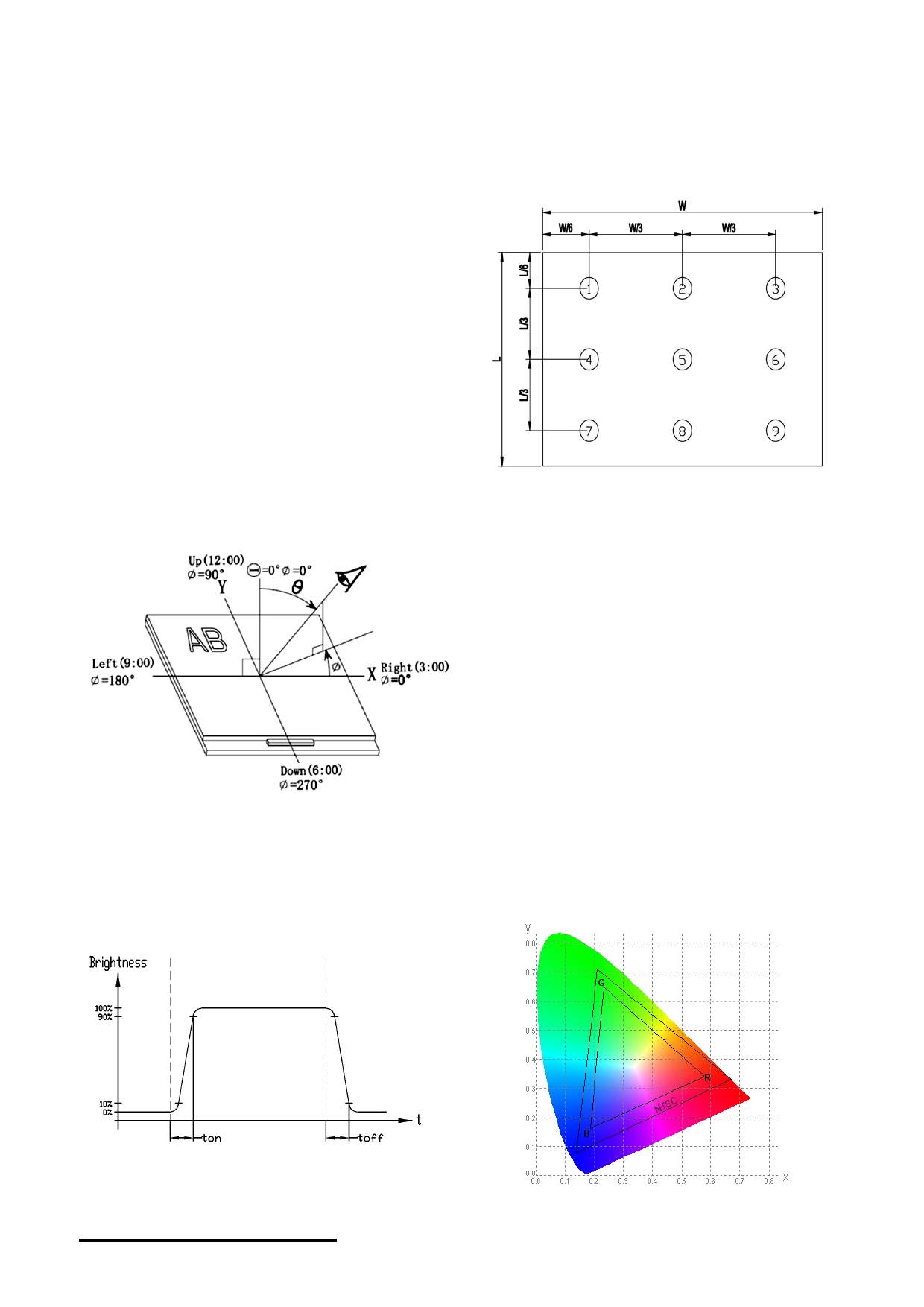
6. TFT Optical Characteristics
200
Note : The parameter is slightly changed by temperature, driving voltage and materiel.
URL: www.topwaydisplay.com
Document Name: LMT035KDH03-NNA-1-Rev0.3
Page: 10 of 22
TOPWAY
LCD Module User Manual
LMT035KDH03-NNA-1
Note 1:
Note 2:
The data are measured after LEDs are turned on for 5 minutes.
The luminance uniformity is calculated by using following
LCM displays full white. The brightness is the average value of 9
formula.
measured spots. Measurement equipment PR-705 (Φ8mm)
△ Bp = Bp (Min.) / Bp (Max.)×100 (%)
Measuring condition:
Bp (Max.) = Maximum brightness in 9 measured spots
- Measuring surroundings: Dark room
- Measuring temperature: Ta=25 ℃ .
Bp (Min.) = Minimum brightness in 9 measured spots .
- Adjust operating voltage to get optimum contrast at the
center of the display.
Measured value at the center point of LCD panel after more than 5
minutes while backlight turning on.
Note 3:
Note 4:
The definition of viewing angle:
The definition of contrast ratio (Test LCM using PR-705):
Refer to the graph below marked by θ and Ф
Luminance When LCD is at “White”
Contrast state
Ratio(CR)= Luminance When LCD is at “Black”
state
(Contrast Ratio is measured in optimum common electrode
voltage)
Note 5:
Note 6:
Definition of Response time. (Test LCD using DMS501):
Definition of Color of CIE Coordinate and NTSC Ratio.
The output signals of photo detector are measured
when the input signals are changed from
Color gamut:
“black” to “white”(falling time)
Area of RGB triangle
and from “white” to “black”(rising time), respectively.
S=
X100%
Area of NTSC triangle
The response time is defined as
the time interval between the 10% and 90% of amplitudes.Refer to
figure as below.
URL: www.topwaydisplay.com
Document Name: LMT035KDH03-NNA-1-Rev0.3
Page: 11 of 22
TOPWAY
LCD Module User Manual
LMT035KDH03-NNA-1
7. Function Specifications
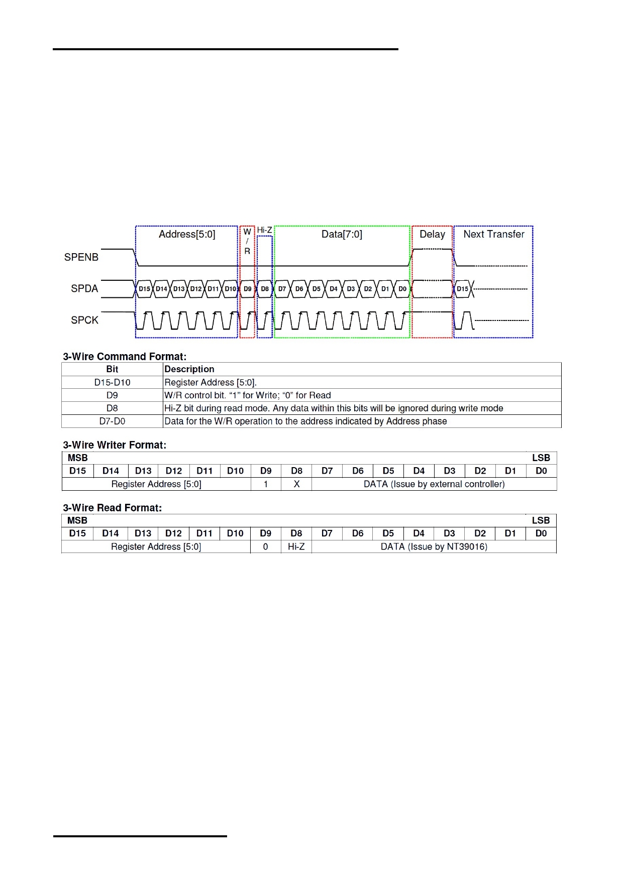
7.1 SPI Interface Command Packet
The LMT035KDH03 terminal equipped with a SPI interface, which is for receiving command to
adjust the TFT display to the best display result.
Command packet is in 16bit format, which include Register Address and Register Data.
/SPEN works as a chip enable pin and also for init the communication.
PSDA is the serial data line
SPCK is the serial clock, data bit latches into the TFT driver at rising edge
URL: www.topwaydisplay.com
Document Name: LMT035KDH03-NNA-1-Rev0.3
Page: 12 of 22
TOPWAY
LCD Module User Manual
LMT035KDH03-NNA-1
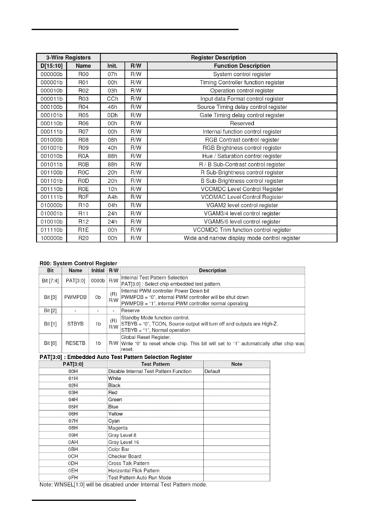
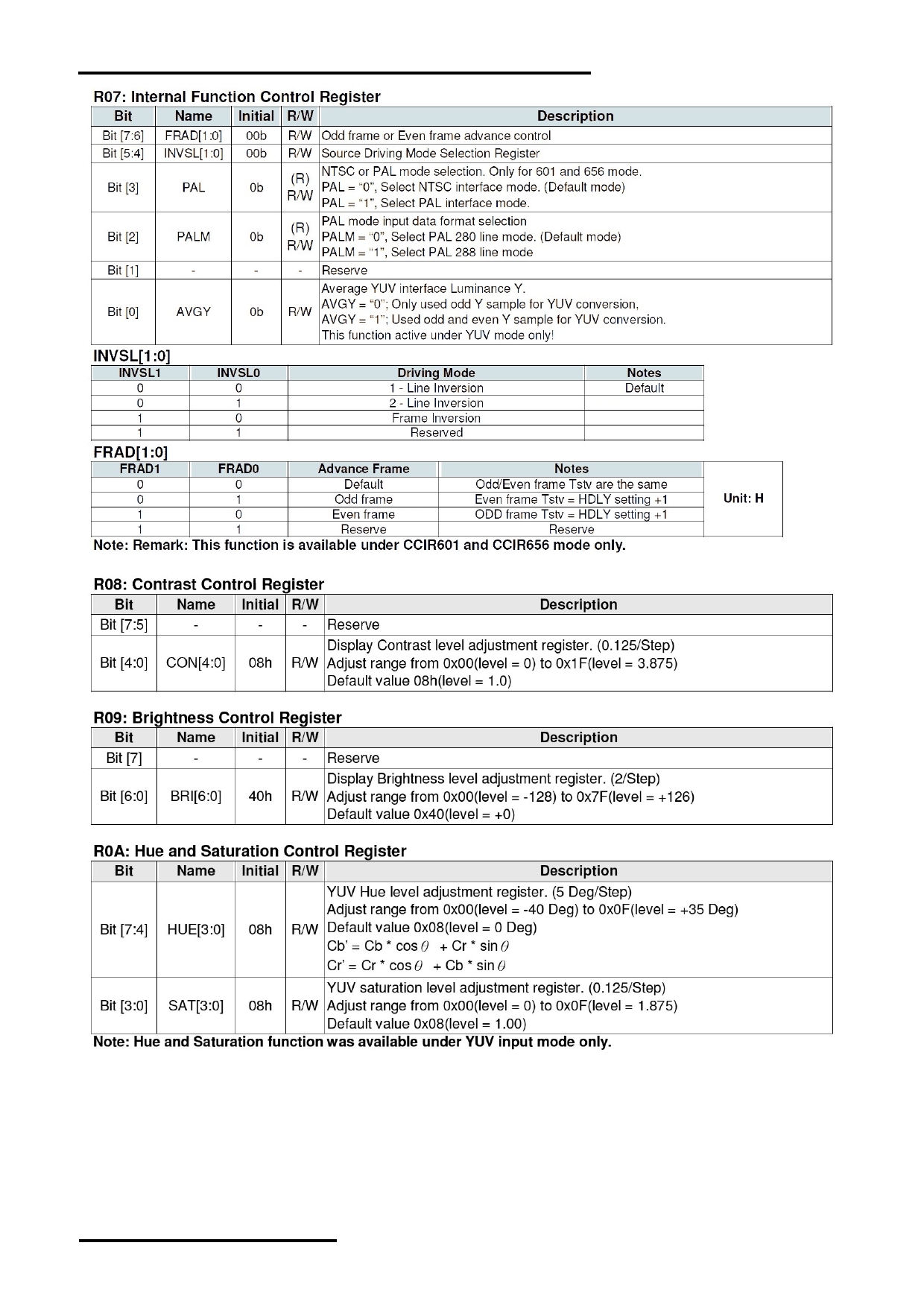
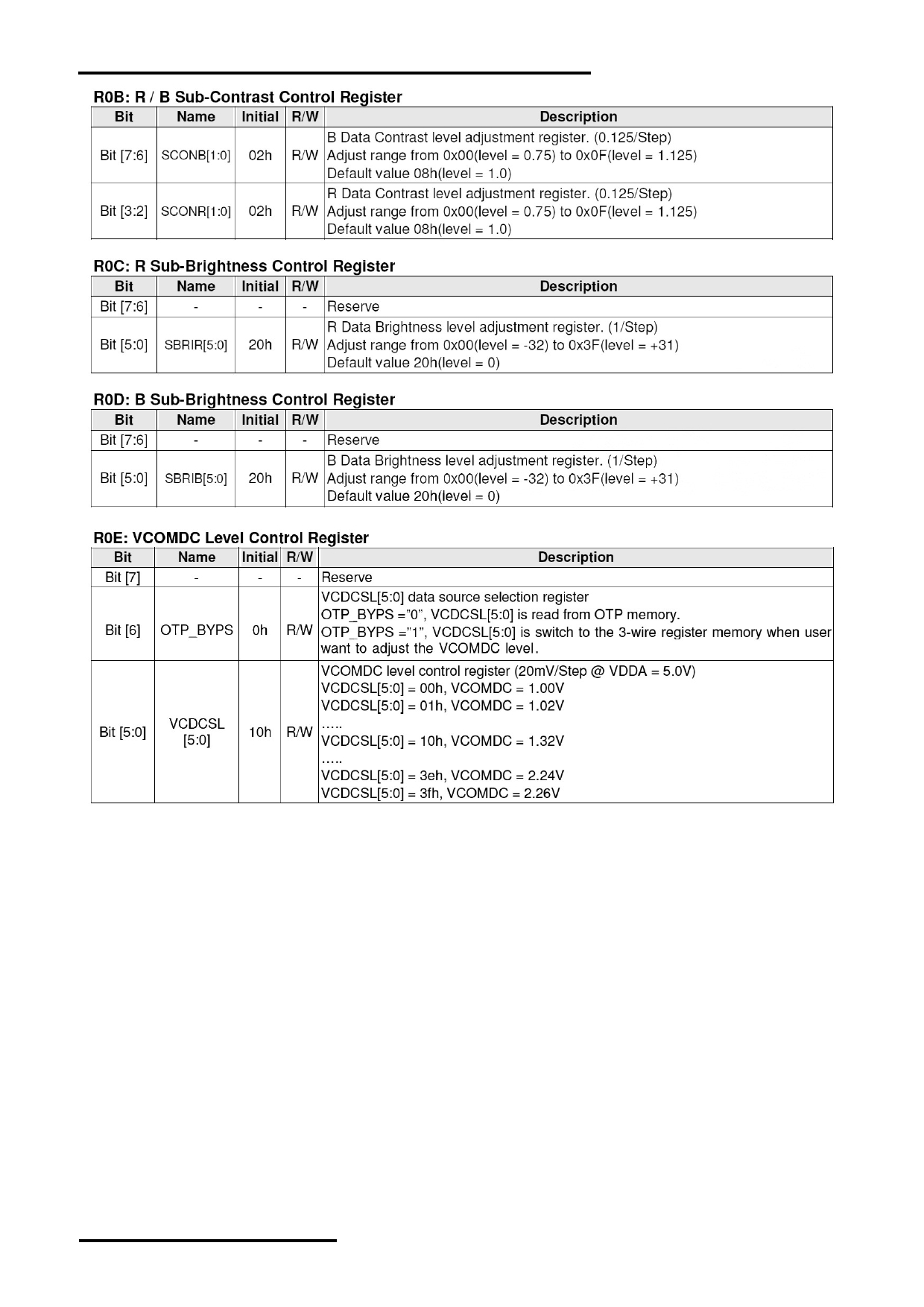
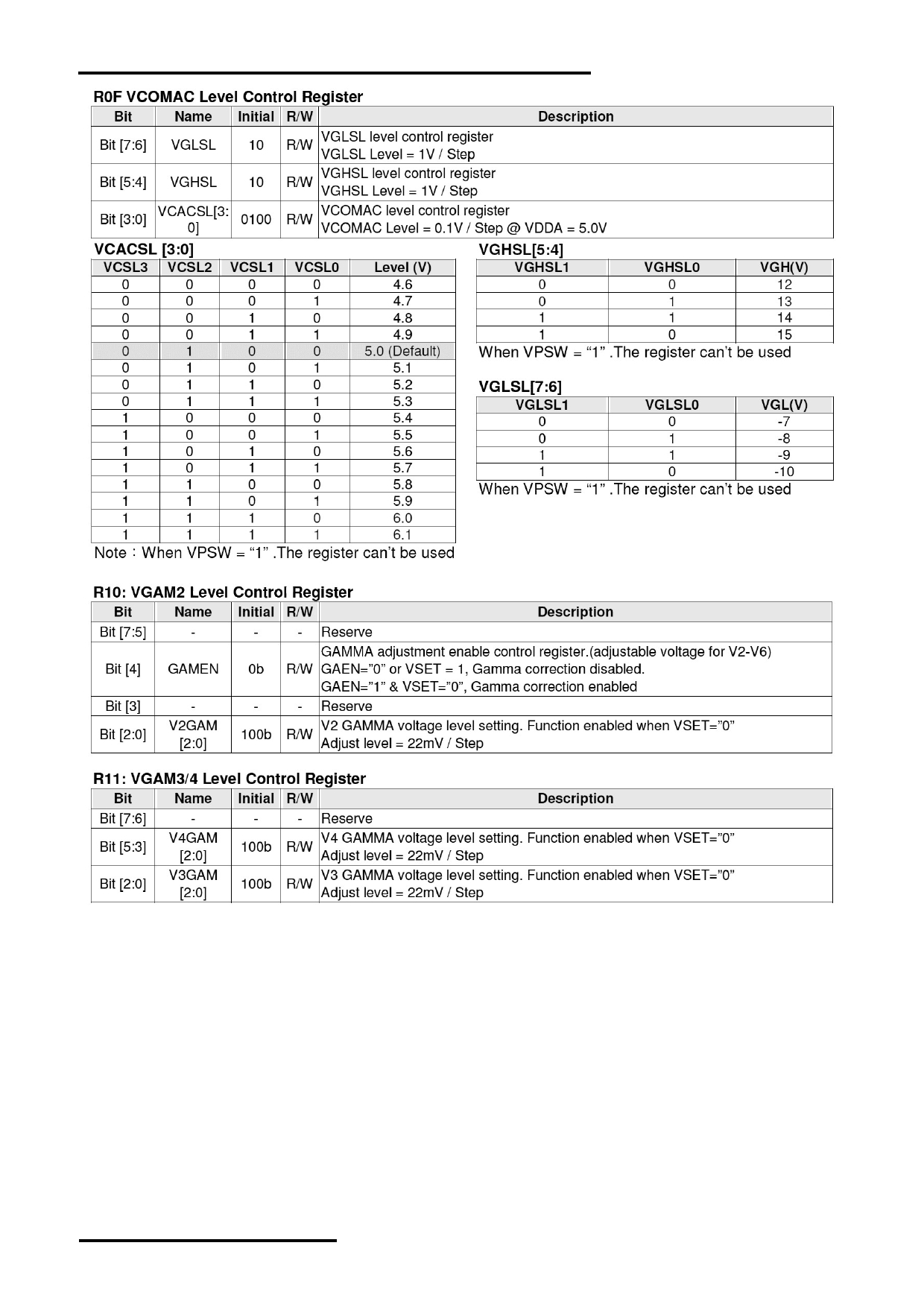
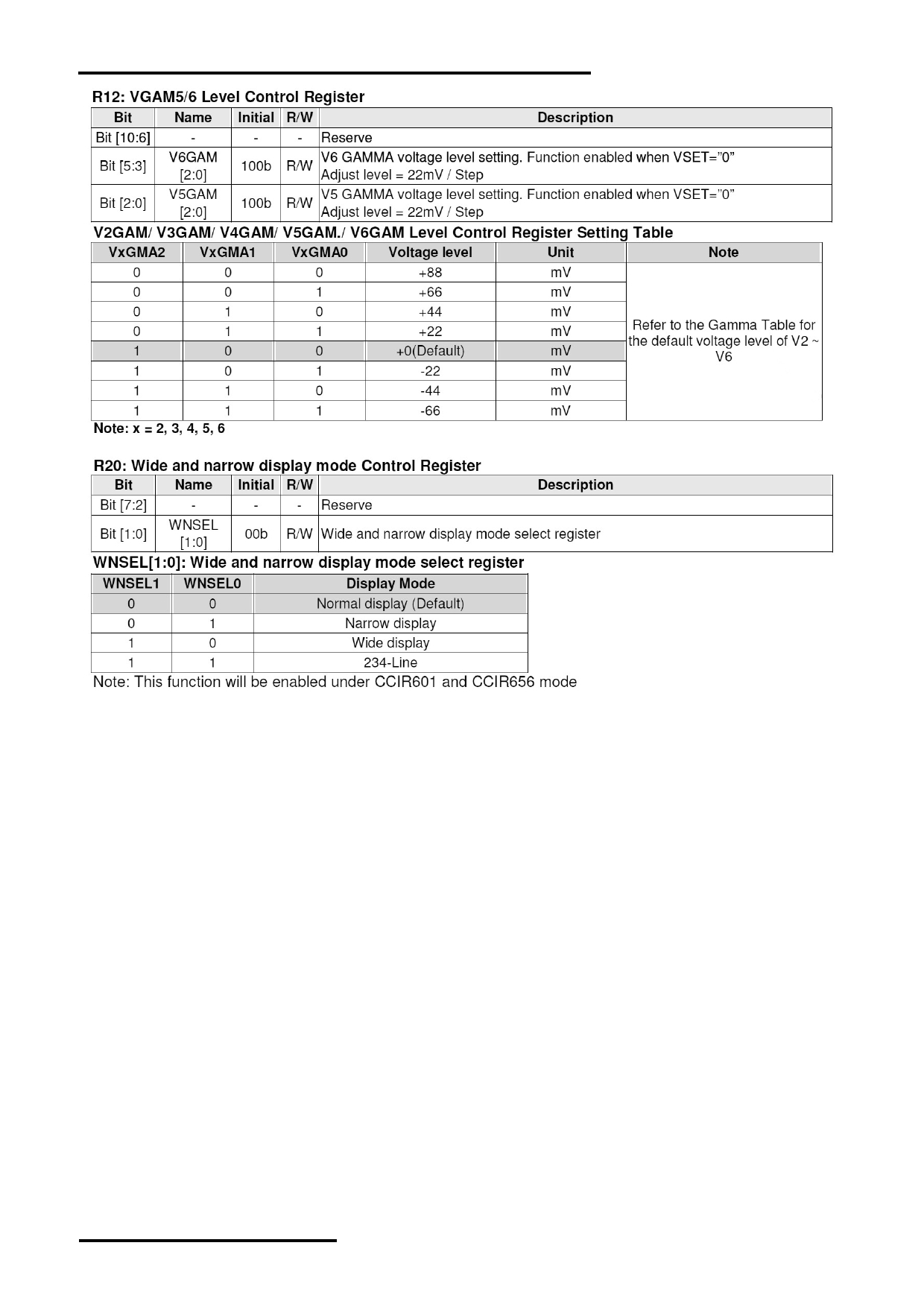
7.2 SPI Interface Commands Summary
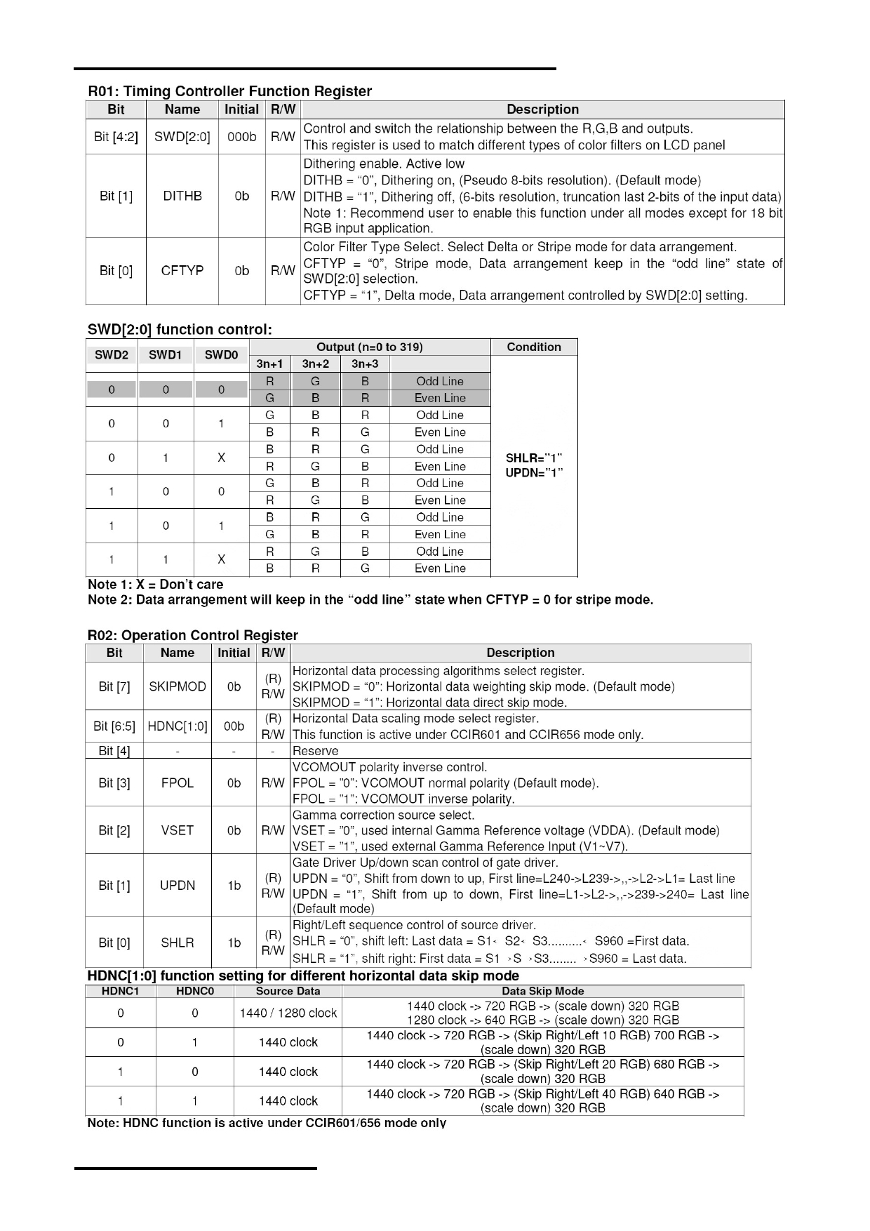
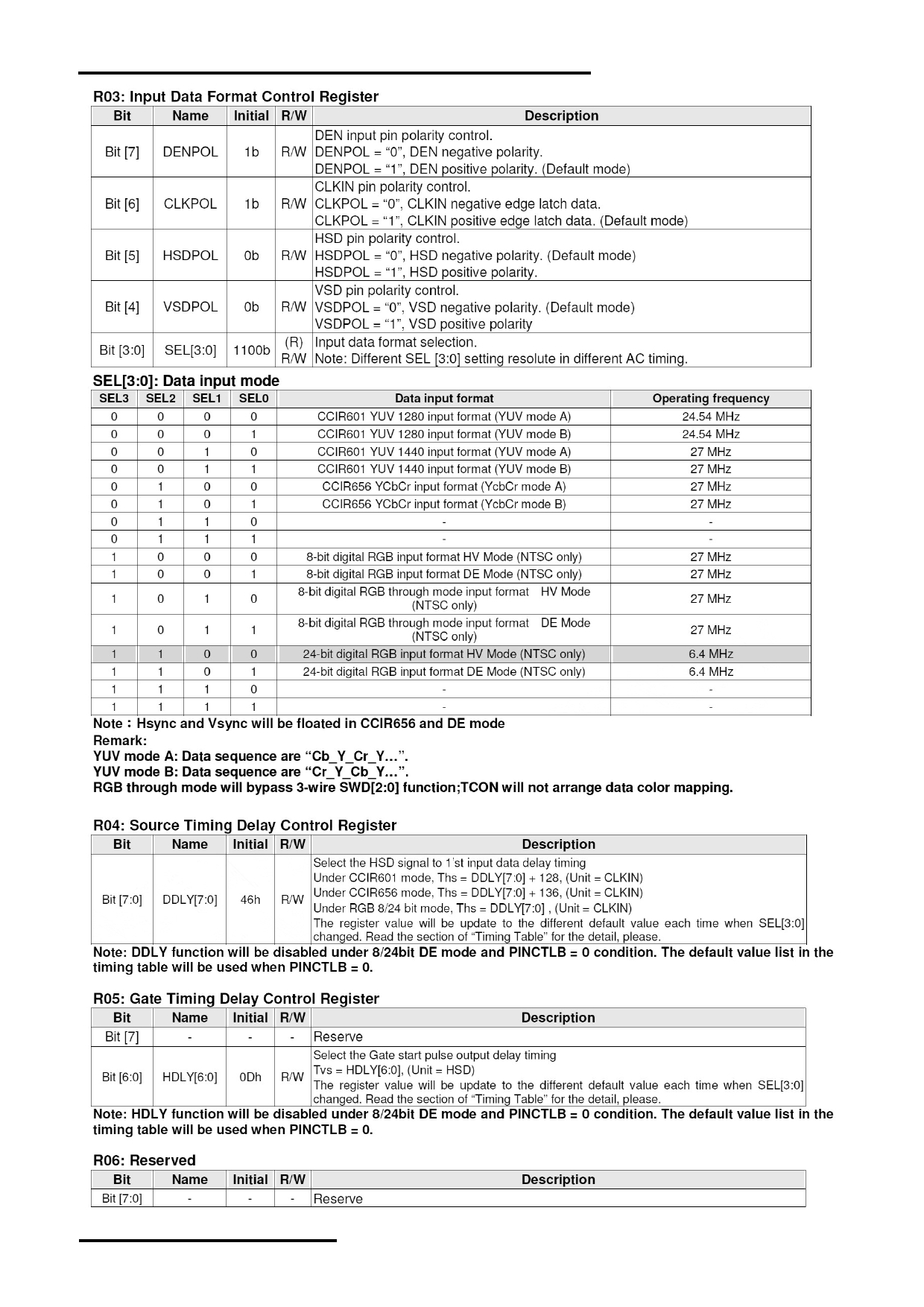
7.3 SPI Interface Commands Details
URL: www.topwaydisplay.com
Document Name: LMT035KDH03-NNA-1-Rev0.3
Page: 13 of 22
TOPWAY
LCD Module User Manual
LMT035KDH03-NNA-1
URL: www.topwaydisplay.com
Document Name: LMT035KDH03-NNA-1-Rev0.3
Page: 14 of 22
TOPWAY
LCD Module User Manual
LMT035KDH03-NNA-1
URL: www.topwaydisplay.com
Document Name: LMT035KDH03-NNA-1-Rev0.3
Page: 15 of 22
TOPWAY
LCD Module User Manual
LMT035KDH03-NNA-1
URL: www.topwaydisplay.com
Document Name: LMT035KDH03-NNA-1-Rev0.3
Page: 16 of 22
TOPWAY
LCD Module User Manual
LMT035KDH03-NNA-1
URL: www.topwaydisplay.com
Document Name: LMT035KDH03-NNA-1-Rev0.3
Page: 17 of 22
TOPWAY
LCD Module User Manual
LMT035KDH03-NNA-1
URL: www.topwaydisplay.com
Document Name: LMT035KDH03-NNA-1-Rev0.3
Page: 18 of 22
TOPWAY
LCD Module User Manual
LMT035KDH03-NNA-1
URL: www.topwaydisplay.com
Document Name: LMT035KDH03-NNA-1-Rev0.3
Page: 19 of 22
TOPWAY
LCD Module User Manual
LMT035KDH03-NNA-1
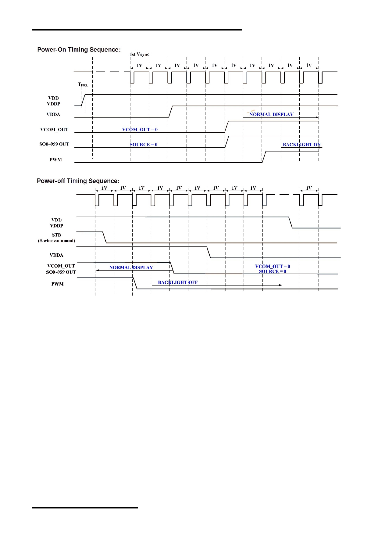
7.4 Power On/Off Sequence
To prevent abnormal display that might show on screen,
it is suggest to use to following standby sequence.
Power on, turn on the backlight AFTER power supply stable and display ready.
Power off, turn off the backlight BEFORE power down.
URL: www.topwaydisplay.com
Document Name: LMT035KDH03-NNA-1-Rev0.3
Page: 20 of 22
TOPWAY
LCD Module User Manual
LMT035KDH03-NNA-1
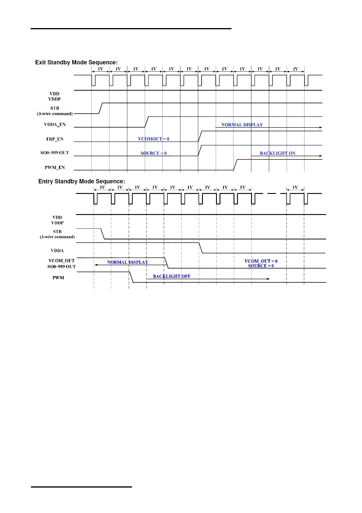
7.5 Standby Sequence
To prevent abnormal display that might show on screen,
it is suggest to use to following standby sequence.
Entering standby mode, turn off the backlight BEFORE standby.
Exiting standby mode, turn on the backlight AFTER exiting standby mode, power supply stable and
display ready.
7.6 Reset Function
To prevent from abnormal reset condition, a glitch filter for RSTB is embedded in this chip. The external reset
signal should keep active for large then reset time (T RSTB ). Refer to the AC/DC Specification for the requirement.
8. Precautions of using LCD Modules
Please refer to "LCD-Module-Design-Handling-Precaution.pdf".
URL: www.topwaydisplay.com
Document Name: LMT035KDH03-NNA-1-Rev0.3
Page: 21 of 22
TOPWAY
LCD Module User Manual
LMT035KDH03-NNA-1
9. Appendix A <Inspection items and criteria for appearance defect>
Items
Criteria
Open Segment or Common
Not permitted
Short
Not permitted
Wrong Viewing Angle
Not permitted
Decliners
Not permitted
Contrast Ration Uneven
According to the limit specimen
Crosstalk
According to the limit specimen
White spots
X>1 pixel
A-area
Not permitted
Max 6 spots
B-area
Max. 1 allowed
1/2 pixel<X≤1 pixel
A-area
Not permitted
allowed
B-area
Max. 2 allowed
X≤1/2 pixel
A-area
Max. 1 allowed
B-area
Max. 4 allowed
Black Sport
X>1 pixel
A-area
Not permitted
B-area
Max. 2 allowed
X≤1/2 pixel
A-area
Max. 1 allowed
B-area
Max. 4 allowed
Line Defect
Apparent vertical horizontal line defects are not permitted
Note:
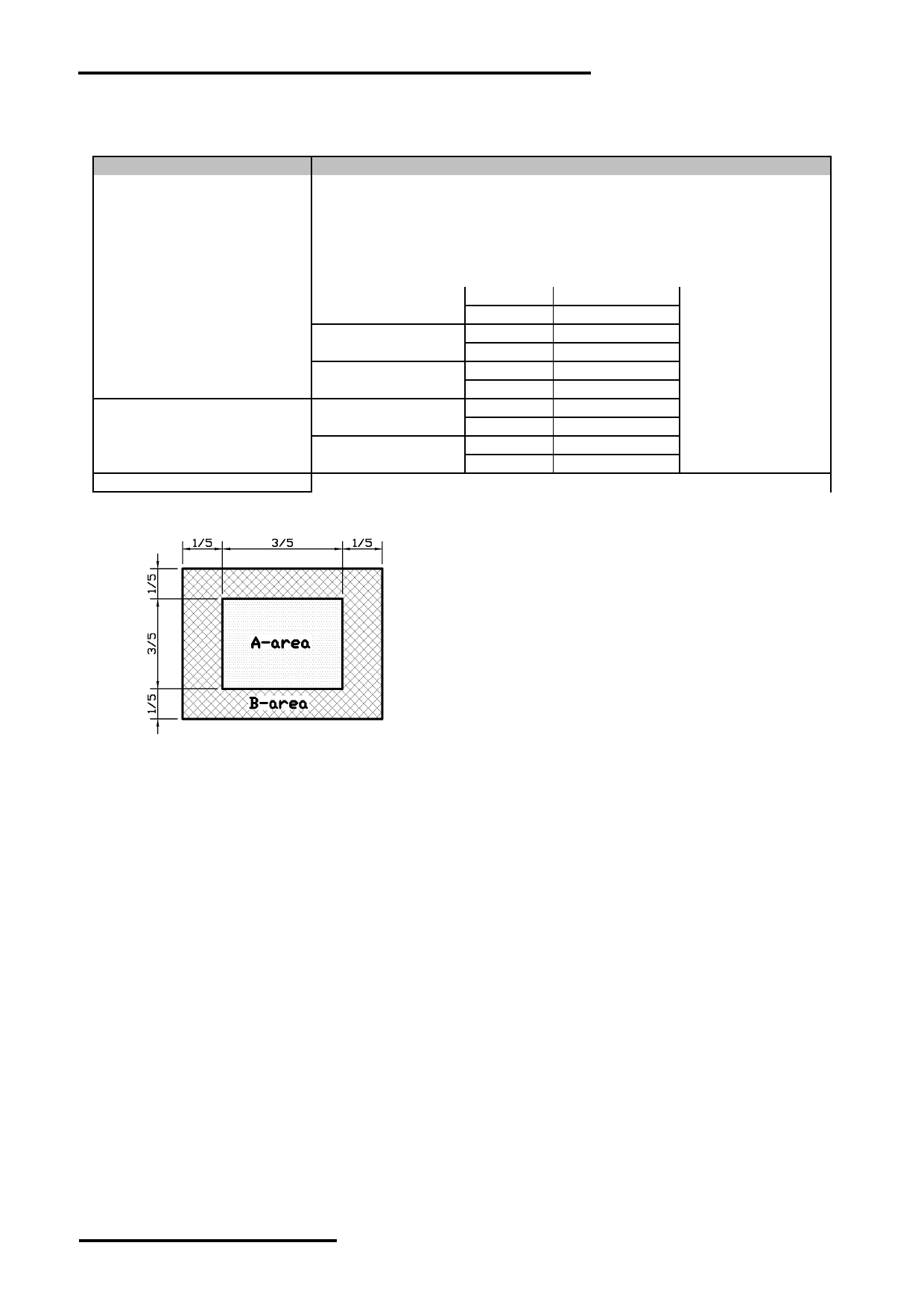
1. On Pixel include 3 dots (RedDot + GreenDot + BlueDot)
2. Definition of Panel “A-area” and “B-area”
URL: www.topwaydisplay.com
Document Name: LMT035KDH03-NNA-1-Rev0.3
Page: 22 of 22