LMT050DNCFWU-NAD
LCD Module User Manual
Prepared by:
Checked by:
Approved by:
Lu jianhui
Date: 2018-08-07
Date:
Date:
Rev. Descriptions
Release Date
0.1
Preliminary new release
2018-08-07
URL: www.topwaydisplay.com
Document Name: LMT050DNCFWU-NAD-Manual-Rev0.1
Page: 1 of 16

TOPWAY
LCD Module User Manual
LMT050DNCFWU-NAD
Table of Content
1. General Specification ............................................................................................................... 3
1.1 Block Diagram .......................................................................................................................... 3
2. Terminal Functions ................................................................................................................... 4
2.1 K1 TFT Driver Terminal ........................................................................................................... 4
3. Absolute Maximum Ratings ..................................................................................................... 4
4. Electrical Characteristics ......................................................................................................... 5
4.1 DC Characteristics ................................................................................................................... 5
4.2 Power ON/OFF Sequence ....................................................................................................... 5
5. AC Characteristics .................................................................................................................... 6
5.1 AC Timing ................................................................................................................................ 6
5.2 Data Input format ..................................................................................................................... 7
5.3 I2C AC Electrical Characteristics .............................................................................................. 8
6. CTP Function Characteristics ................................................................................................. 9
6.1 Initialization .............................................................................................................................. 9
6.2 I2C Slave Interface................................................................................................................... 9
6.3 Register Read .......................................................................................................................... 9
6.4 Register Write ........................................................................................................................ 10
6.5 I2C Electrical Waveform ......................................................................................................... 10
6.6 Report Page Registers ........................................................................................................... 11
7. Optical Characteristics .......................................................................................................... 13
8. Precautions of using LCD Modules ...................................................................................... 15
URL: www.topwaydisplay.com
Document Name: LMT050DNCFWU-NAD-Manual-Rev0.1
Page: 2 of 16
TOPWAY
LCD Module User Manual
LMT050DNCFWU-NAD
1. General Specification
Screen Size(Diagonal) :
5.0 inch
Resolution :
800 x 480
Signal Interface :
24bit parallel interface
Color Depth :
16.7M color
Pixel Pitch :
0.135 x 0.135 (mm)
Pixel Configuration :
RGB Stripe
Display Mode :
Transmissive / normal white
Surface Treatment :
HC Treatment
Viewing Direction :
6H (*1) (gray scale inverse)
12H (*2)
Outline Dimension :
121.3 x 76.4 x 8.3 (mm)
(see attached drawing for details)
Active Area :
108 x 64.8 (mm)
Operating Temperature :
-20 ~ +70°C
Storage Temperature :
-30 ~ +80°C
Note:
*1. For saturated color display content (eg. pure-red, pure-green, pure-blue, or pure-colors-combinations).
*2. For “color scales” display content.
*3. Color tone may slightly change by Temperature and Driving Condition.
1.1 Block Diagram
TPSDA,TPSCL
/TPRST, /TPINT
Capacitive Touch Panel
R0~R7, G0~G7, B0~B7
800 x 480 pixels
DCLK, HS, VS, /STBY
B
TFT Panel
BLADJ, BLEN
Backlight Circuit
+5V,GND
Power Supply Circuit
URL: www.topwaydisplay.com
Document Name: LMT050DNCFWU-NAD-Manual-Rev0.1
Page: 3 of 16
TOPWAY
LCD Module User Manual
LMT050DNCFWU-NAD
2. Terminal Functions
2.1 K1 TFT Driver Terminal
Pin Pin
No. Name
I/O
Descriptions
1
5V
:
:
Power
5V power supply
5
5V
6
GND
:
:
Power
0V power supply
10
GND
11
BLADJ
Input
Backlight brightness PWM signal (active low)
12
BLEN
Input
Backlight enable signal (active high)
13
NC(MODE) NC
No Connection
14
NC(DE)
NC
No Connection
15
VS
Input
Vertical sync signal
16
HS
Input
Horizontal sync signal
17
B7
:
:
Input
Blue data line
24
B0
25
G7
:
:
Input
Green data line
32
G0
33
R7
:
:
Input
Red data line
40
R0
41
GND
Power
Ground, 0V
42
DCLK
Input
Pixel clock
43
GND
Power
Ground, 0V
44
/STBYB
Input
STBYB signal (pull hi for normal operation)
45
GND
Power
Ground, 0V
46
/TPRST
Input
Reset signal, active low reset
47
/TPINT
Output
Interrupt signal, active low interrupt
48
TPSDA
I/O
I 2 C data (*1)
49
TPSCL
Input
I 2 C clock (*1)
50
GND
Power
Ground
Note:
*1. With internal resister(4.7k) pull up.
3. Absolute Maximum Ratings
Items
Symbol
Min.
Max.
Unit
Condition
Power Voltage
V 5V
-0.3
+6
V
GND = 0V
Operating Temperature
T OP
-20
+70
℃
No Condensation
Storage Temperature
T ST
-30
+80
℃
No Condensation
Cautions:
Any Stresses exceeding the Absolute Maximum Ratings may cause substantial damage to the device. Functional
operation of this device at other conditions beyond those listed in the specification is not implied and prolonged exposure
to extreme conditions may affect device reliability.
URL: www.topwaydisplay.com
Document Name: LMT050DNCFWU-NAD-Manual-Rev0.1
Page: 4 of 16
TOPWAY
LCD Module User Manual
LMT050DNCFWU-NAD
4. Electrical Characteristics
4.1 DC Characteristics
GND=0V, V 5V =5.0V, T OP =25 ℃
Items
Symbol
MIN.
TYP.
MAX.
Unit Applicable Pin
Power Voltage
V 5V
4.5
5.0
5.5
V
5V
Operating Current (*1)
I 5V
-
260
400
mA
Input High Voltage
V IH
3.0
-
3.3
V
Input pins
Input Low Voltage
V IL
0
-
0.3
V
Input pins
Output Signal High Voltage
V oH
3.0
-
3.6
V
Output Signal Low Voltage
V oL
0
-
0.6
V
Note.
*1. For different LCM, the value may have a bit of difference.
*2. To test the current dissipation, use “all Black Pattern”.
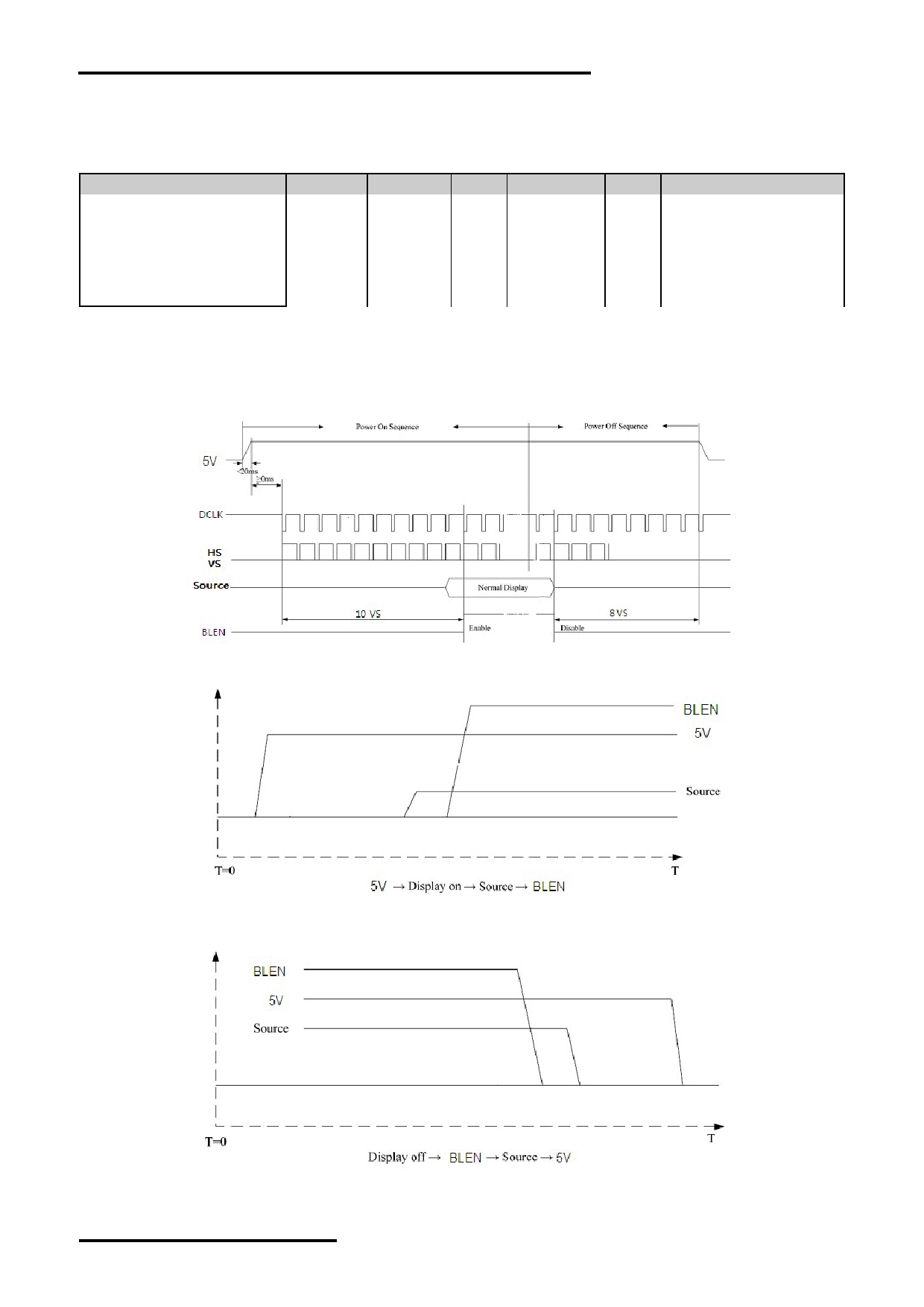
4.2 Power ON/OFF Sequence
Power On/Off Sequence
Power On Sequence
Power OFF Sequence
URL: www.topwaydisplay.com
Document Name: LMT050DNCFWU-NAD-Manual-Rev0.1
Page: 5 of 16
TOPWAY
LCD Module User Manual
LMT050DNCFWU-NAD
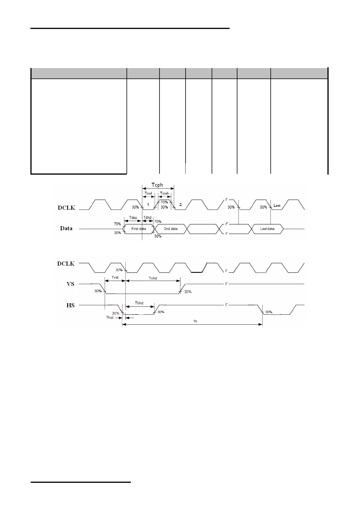
5. AC Characteristics
5.1 AC Timing
GND=0V, V 5V =5.0V, T OP =25 ℃
Item
Symbol
MIN.
TYP.
MAX.
Unit
Remark
HS setup time
Thst
8
-
-
ns
HS hold time
Thhd
8
-
-
ns
VS setup time
Tvst
8
-
-
ns
VS hold time
Tvhd
8
-
-
ns
Data setup time
Tdsu
8
-
-
ns
Data hole time
Tdhd
8
-
-
ns
DE setup time
Tesu
8
-
-
ns
DCLK cycle time
Tcph
20
-
-
ns
DCLK pulse duty
Tcwh
40
50
60
%
Input Clock and Data Timing Diagram
URL: www.topwaydisplay.com
Document Name: LMT050DNCFWU-NAD-Manual-Rev0.1
Page: 6 of 16
TOPWAY
LCD Module User Manual
LMT050DNCFWU-NAD
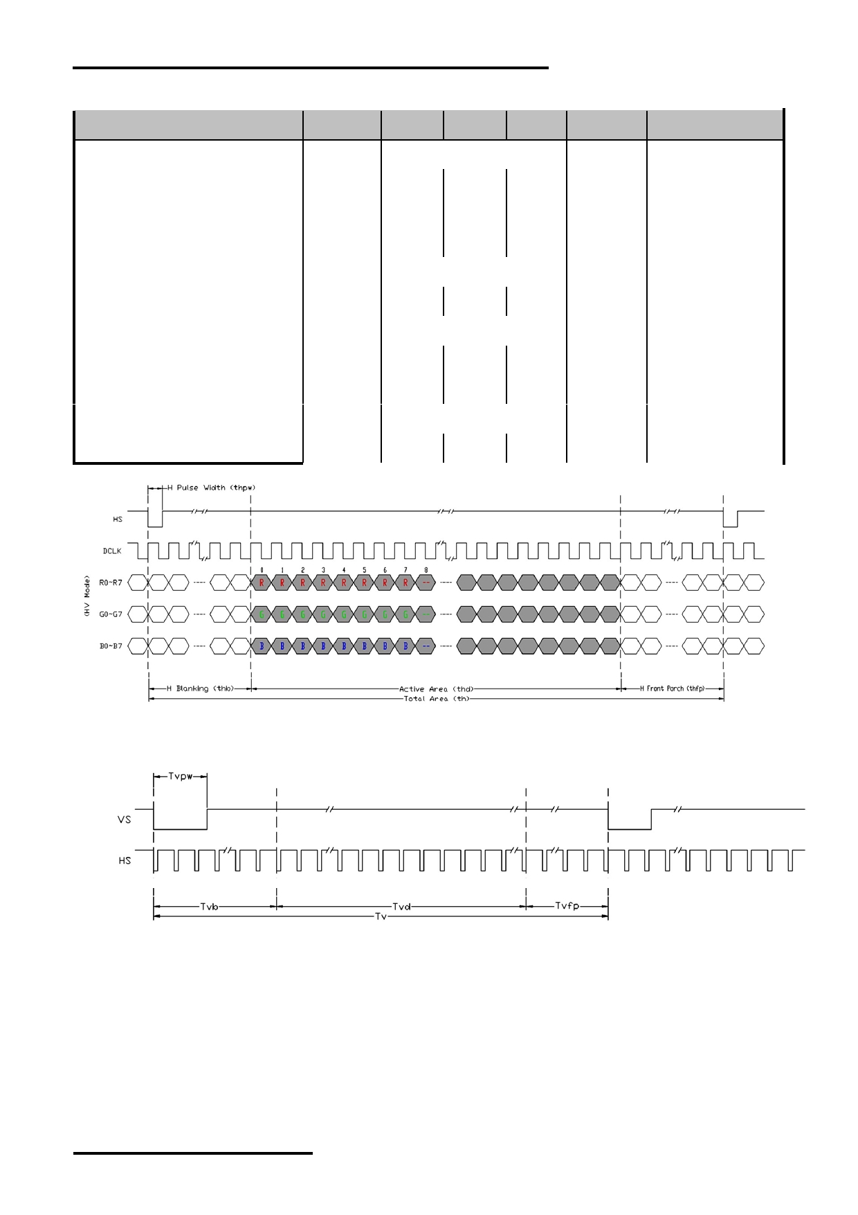
5.2 Data Input format
Item
Symbol
MIN.
TYP.
MAX.
Unit
Remark
Horizontal Display Area
thd
800
DCLK
DCLK Frequency
fclk
-
30
50
MHz
One Horizontal Line
th
889
928
1143
DCLK
HS pulse width
thpw
1
48
255
DCLK
HS Blanking
thb
88
DCLK
HS Front Porch
thfp
1
40
255
DCLK
Vertical Display Area
tvd
480
TH
VS period time
tv
513
525
767
TH
VS pulse width
tvpw
3
3
255
TH
VS Blanking
tvb
32
TH
VS Front Porch
tvfp
1
13
255
TH
Horizontal input timing diagram
Vertical input timing diagram
URL: www.topwaydisplay.com
Document Name: LMT050DNCFWU-NAD-Manual-Rev0.1
Page: 7 of 16
TOPWAY
LCD Module User Manual
LMT050DNCFWU-NAD
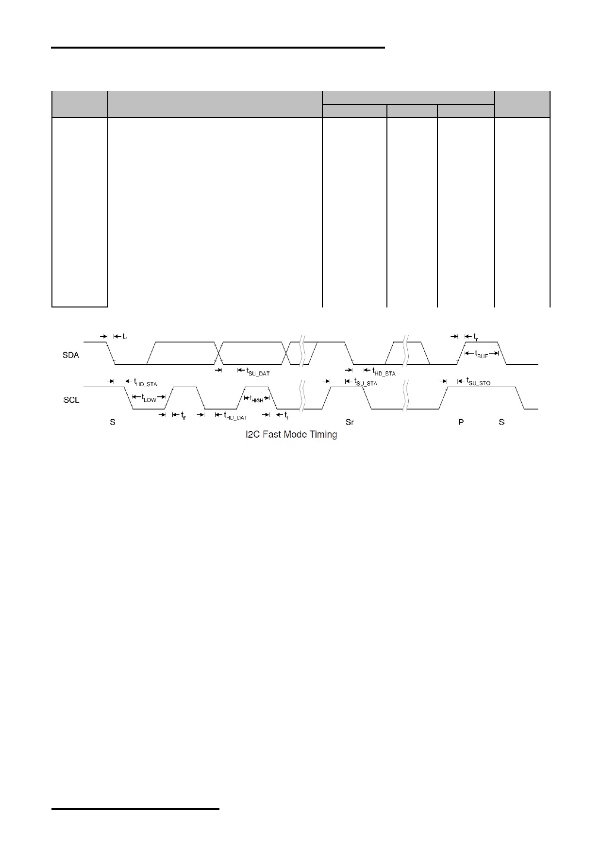
5.3 I2C AC Electrical Characteristics
GND=0V, V 5V =5.0V, T OP =25 ℃
Symbol
Parameter
Rating
Min.
Typ.
Max.
Unit
f SCL
SCL clock frequency
0
-
400
kHz
t LOW
Low period of the SCL clock
1.3
-
-
us
t HIGH
High period of the SCL clock
0.6
-
-
us
t f
Signal falling time
-
-
300
us
t r
Signal rising time
-
-
300
us
t SU_STA
Set up time for a repeated START
condition
0.6
-
-
us
Hold time (repeated) START condition.
t HD_STA
After this period, the first clock pulse is
0.6
-
-
us
generated
t SU_DAT
Data set up time
100
-
-
us
t HD_DAT
Data hold time
0
-
0.9
us
t SU_STO
Set up time for STOP condition
0.6
-
-
us
t BUF
Bus free time between a STOP and
START condition
1.3
-
-
us
URL: www.topwaydisplay.com
Document Name: LMT050DNCFWU-NAD-Manual-Rev0.1
Page: 8 of 16
TOPWAY
LCD Module User Manual
LMT050DNCFWU-NAD
6. CTP Function Characteristics
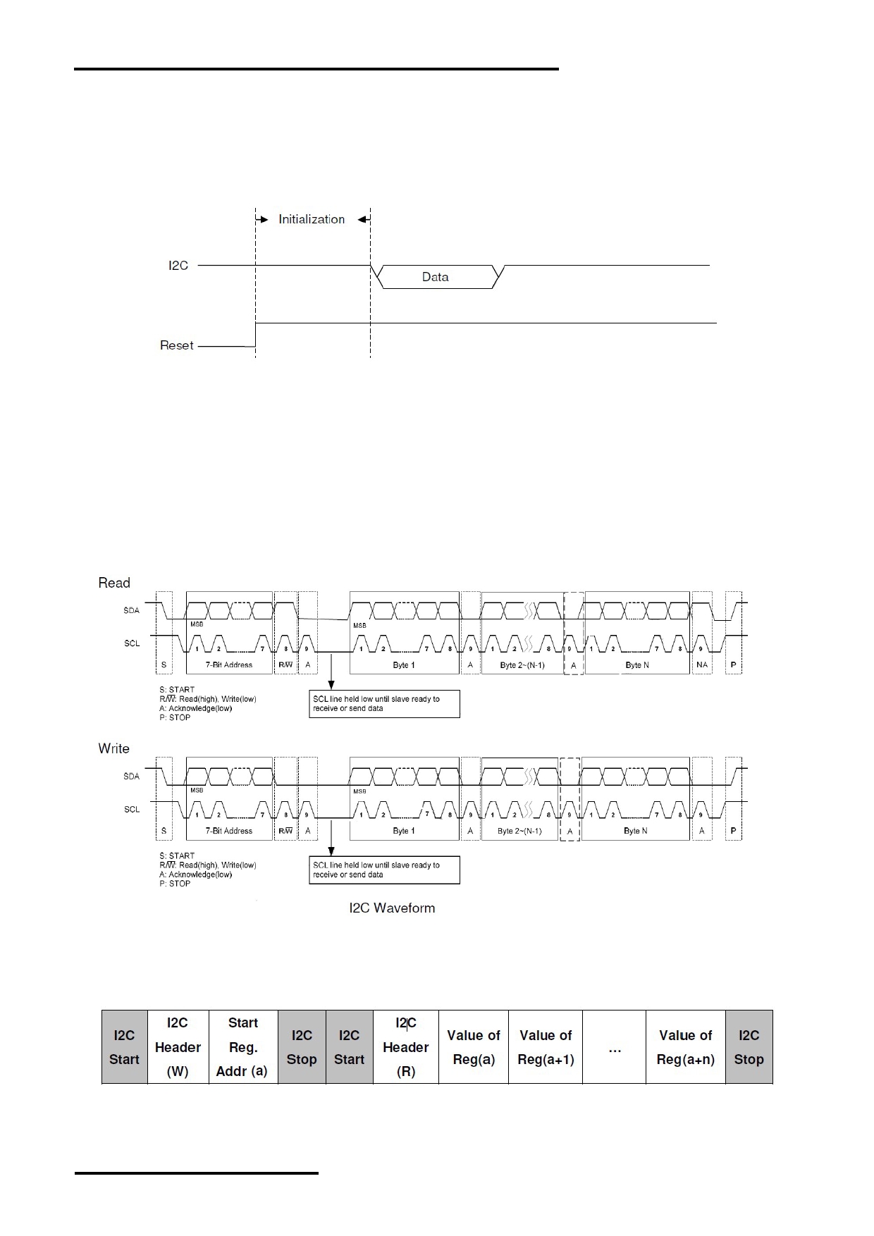
6.1 Initialization
After hardware reset, touch controller needs some time for initialization. The touch controller can be
accessed via I2C interface after initialization. Initialization time is 50ms.
6.2 I2C Slave Interface
Touch IC equipped with I2C provides two wires, serial data (SDA) and serial clock (SCL), to carry
transferring information at up to 400 kbit/s(Fast mode). I2C address is default to 0x55 (7-bits address).
Touch IC plays the slave role in I2C transfer. Both SDA and SCL are bidirectional lines, connected to IOVDD
via pull-up resistors. All transactions begin with a START (S) and can be terminated by a STOP (P). 7-bits
address follows START to recognize device. Each bye is 8-bits length and followed by an acknowledge bit. A
HIGH to LOW transition on the SDA line while SCL is HIGH defines a START condition. A LOW to HIGH
transition on the SDA line while SCL is HIGH defines a STOP condition. The data on the SDA line must be
stable during the HIGH period of the clock. The HIGH or LOW state of the data line can only change when
the clock signal on the SCL line is LOW.
6.3 Register Read
For reading register value from I2C device, host has to tell I2C device the Start Register Address before
reading corresponding register value.
Register Read Format
URL: www.topwaydisplay.com
Document Name: LMT050DNCFWU-NAD-Manual-Rev0.1
Page: 9 of 16
TOPWAY
LCD Module User Manual
LMT050DNCFWU-NAD
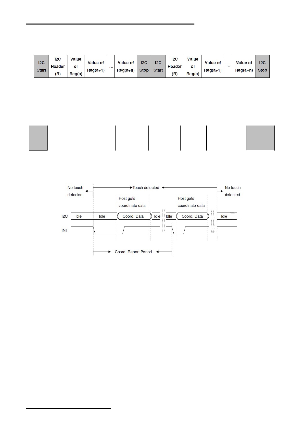
I2C host interface protocol supports Repeated Register Read. That is, once the Start Register Address has
been set by host, consequent I2C Read(R) transactions will directly read register values starting from the
Start Register Address without setting address first, as shown in Repeated Register Read.
Repeated Register Read
6.4 Register Write
For writing register to I2C device, host has to tell I2C device the Start Register Address in each I2C Register
Write transaction. Register values to the I2C device will be written to the address starting from the Start
Register Address described in Register Write I2C transaction as shown in Register Write Format .
I2C
I2C
Start Reg.
Value to
Value to
Value to
I2C
Start Header(W)
Addr.(a)
Reg(a)
Reg(a+1)
…
Reg(a+n)
Stop
Register Write Format
6.5 I2C Electrical Waveform
URL: www.topwaydisplay.com
Document Name: LMT050DNCFWU-NAD-Manual-Rev0.1
Page: 10 of 16
TOPWAY
LCD Module User Manual
LMT050DNCFWU-NAD
6.6 Report Page Registers
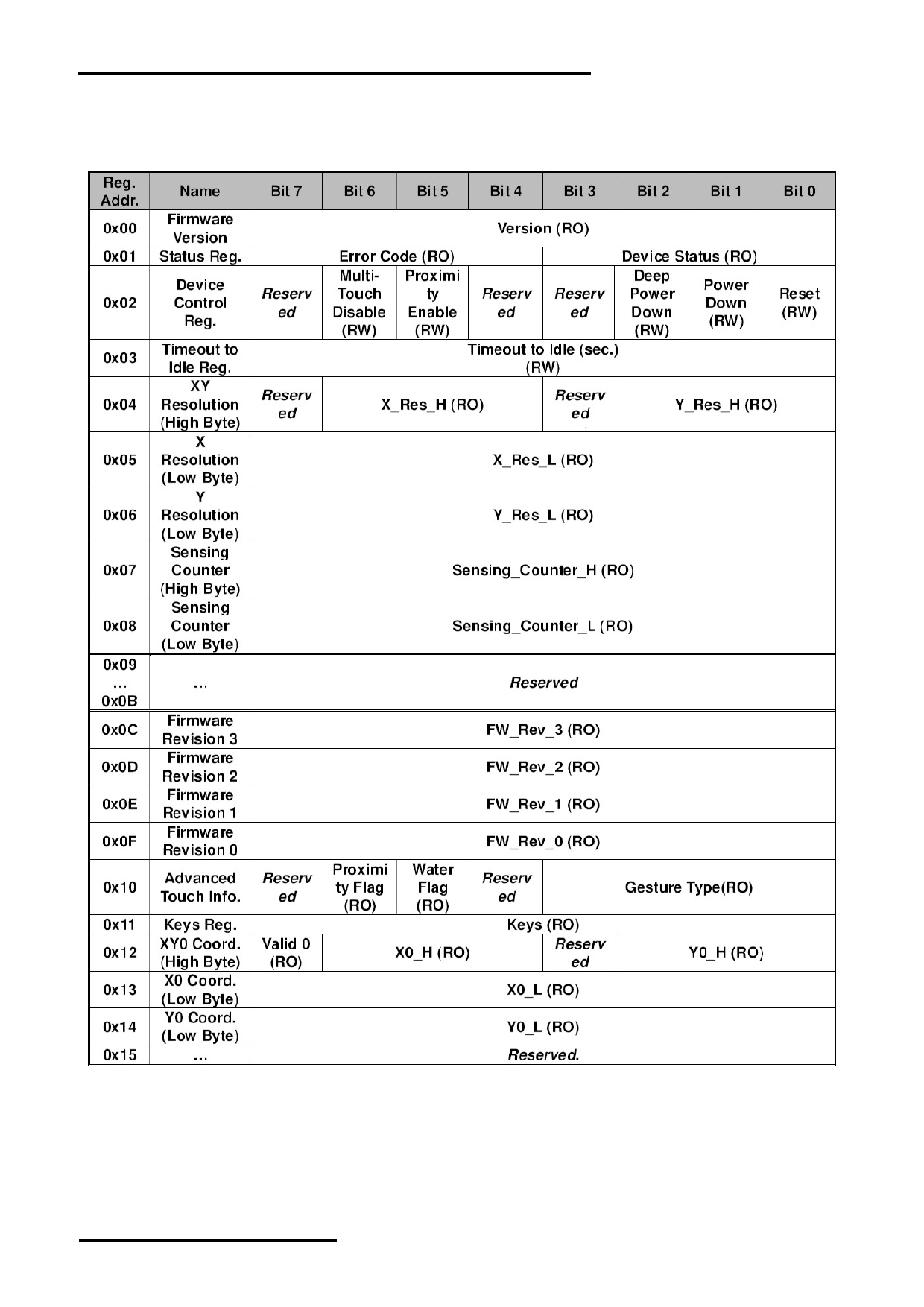
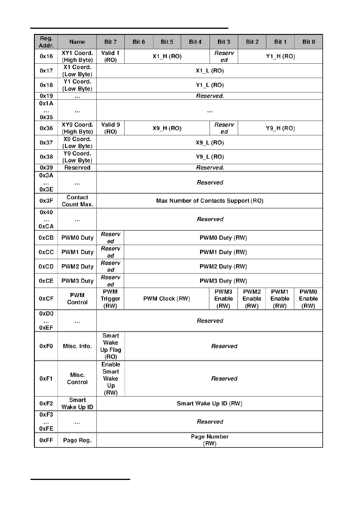
Touch IC provides a register set for host to configure device attributes and retrieve information about
fingers and raw data through device host interface. Host interface registers are listed below.
URL: www.topwaydisplay.com
Document Name: LMT050DNCFWU-NAD-Manual-Rev0.1
Page: 11 of 16
TOPWAY
LCD Module User Manual
LMT050DNCFWU-NAD
Note:
Please refer to ST1633i IC datasheet and Sitronix Touch IC Protocol for detail.
URL: www.topwaydisplay.com
Document Name: LMT050DNCFWU-NAD-Manual-Rev0.1
Page: 12 of 16
TOPWAY
LCD Module User Manual
LMT050DNCFWU-NAD
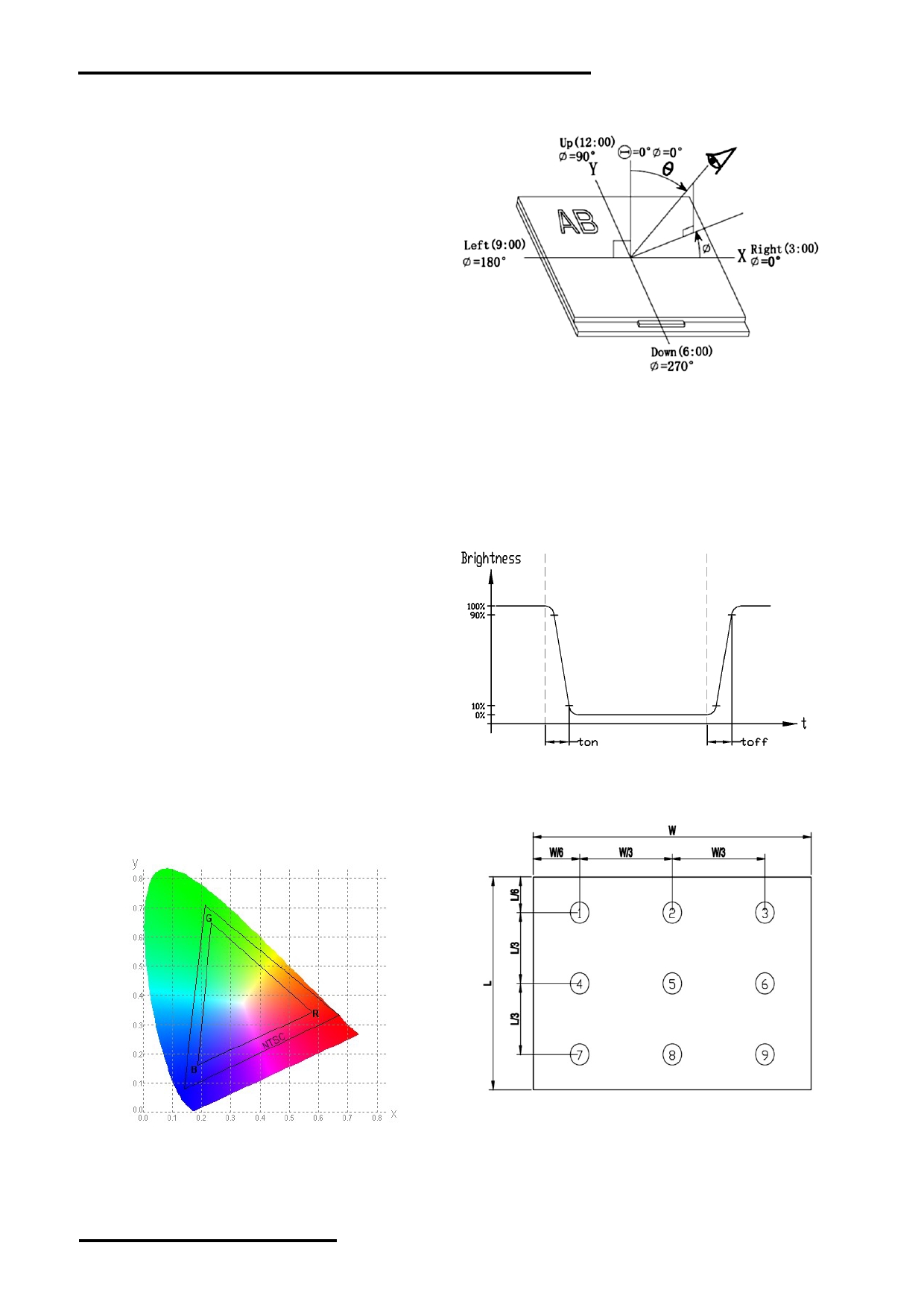
7. Optical Characteristics
Item
Symbol
Condition
MIN.
TYP.
MAX.
UNIT
Note.
θ T
40
50
-
Viewing angle
θ B
60
70
-
(CR ≥ 10)
degree
Note 2
θ L
60
70
-
θ R
60
70
-
Contrast ratio
CR
θ=0 o
500
600
-
-
Note 1,3
T on
msec
Response Time
25 ℃
-
20
30
Note 1,4
T off
msec
X
0.260 0.310 0.360
White
Y
0.280 0.330 0.380
X
0.540 0.590 0.640
Red
Y
Backlight
0.300 0.350 0.400
Chromaticlty
is on
Note 1,5
X
0.298 0.348 0.398
Green
Y
0.520 0.570 0.620
X
0.095 0.145 0.195
Blue
Y
0.060 0.110 0.160
Luminance
L
-
200
-
cd/m 2
Note 1,6
NTSC
-
50
%
Note 5
Luminance uniformity
U
75
80
-
%
Note 1,7
Test Conditions:
1. IF= 40mA, VF=21.7V, and the ambient temperature is 25. ℃
2. The test systems refer to Note 1 and Note 2.
URL: www.topwaydisplay.com
Document Name: LMT050DNCFWU-NAD-Manual-Rev0.1
Page: 13 of 16
TOPWAY
LCD Module User Manual
LMT050DNCFWU-NAD
Note 1:
Note 2:
The data are measured after LEDs are turned on for 5 minutes.
The definition of viewing angle:
LCM displays full white. The brightness is the average value of 9 Refer to the graph below marked by θ and Ф
measured spots. Measurement equipment SR-3A (1°)
Measuring condition:
- Measuring surroundings: Dark room
- Measuring temperature: Ta=25 ℃ .
- Adjust operating voltage to get optimum contrast at
the center of the display.
Note 3:
The definition of contrast ratio (Test LCM using SR-3A (1°)):
Note 4:
Contrast
Luminance When LCD is at “White” state
Definition of Response time. (Test LCD using BM-7A(2°)):
Ratio(CR)
=
Luminance When LCD is at “Black” state
The output signals of photo detector are measured
(Contrast Ratio is measured in optimum common electrode
when the input signals are changed from
voltage)
“black” to “white”(falling time)
and from “white” to “black”(rising time), respectively.
The response time is defined as
the time interval between the 10% and 90% of amplitudes.Refer to
figure as below.
Note 5:
Note 6:
Definition of Color of CIE1931 Coordinate and NTSC Ratio.
The luminance uniformity is calculated by using following formula.
△ Bp = Bp (Min.) / Bp (Max.)×100 (%)
Color gamut:
Bp (Max.) = Maximum brightness in 9 measured spots
Area of RGB triangle
S=
X100%
Bp (Min.) = Minimum brightness in 9 measured spots .
Area of NTSC triangle
Note 7:
Measured the luminance of white state at center point
URL: www.topwaydisplay.com
Document Name: LMT050DNCFWU-NAD-Manual-Rev0.1
Page: 14 of 16
TOPWAY
LCD Module User Manual
LMT050DNCFWU-NAD
8. Precautions of using LCD Modules
Please refer to "LCD-Module-Design-Handling-Precaution.pdf".
附录一:
CTP Application Precautions
1. CTP Mounting Precaution
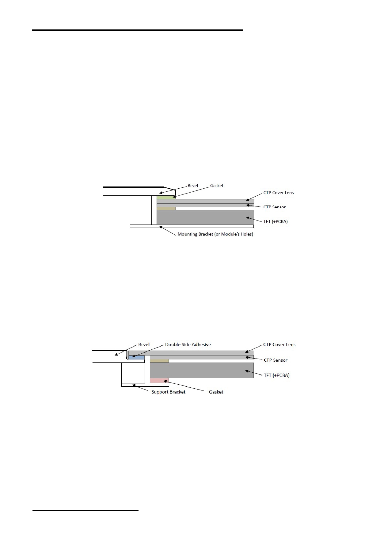
1.1 Bezel Mounting (Figure 1)
- The bezel window should be bigger than the CTP active area. It should be ≥ 0.5mm each side.
- Gasket should be installed between the bezel and the CTP surface.
The final gap should be about 0.5~1.0mm.
- It is recommended to provide an additional support bracket for backside support when
necessary (e.g. slim type TFT module without mounding structure). They should only provide
appropriate support and keep the module in place.
- The mounting structure should be strong enough to prevent external uneven force or twist act
onto the module.
Figure 1
1.2 Surface Mounting (Figure 2)
- As the CTP assembling on the countersink area with double side adhesive.
The countersink area should be flat and clean to ensure the double side adhesive installation
result.
- The Bezel is recommend to keep a gap ( ≥ 0.3mm each side) around the cover lens for
tolerance.
- It is recommended to provide an additional support bracket with gasket for backside support
when necessary (e.g. TFT module without mounding structure). They should only provide
appropriate support and keep the module in place.
- The mounting structure should be strong enough to prevent external uneven force or twist act
onto the module.
Figure 2
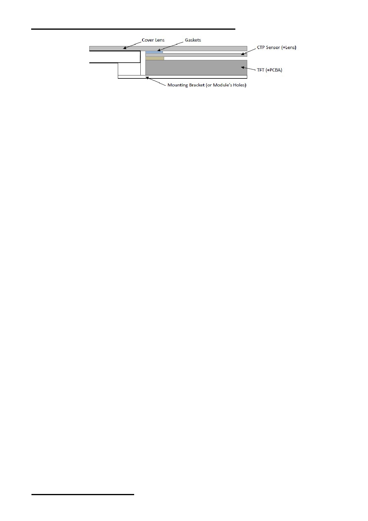
1.3 Additional Cover Lens Mounting (Figure 3)
- For the case of additional cover Lens mounting, it is necessary to recheck with the CTP
specification about the material and thickness to ensure the functionality.
- It should keep a 0.2~0.3mm gap between the cover lens and the CTP surface..
- The cover lens window should be bigger than the active area of the CTP.
It should be ≥ 0.5mm each side.
- It is recommended to provide an additional support bracket for backside support when
necessary (e.g. slim type TFT module without mounding structure). They should only provide
appropriate support and keep the module in place.
- The mounting structure should be strong enough to prevent external uneven force or twist act
onto the module.
URL: www.topwaydisplay.com
Document Name: LMT050DNCFWU-NAD-Manual-Rev0.1
Page: 15 of 16
TOPWAY
LCD Module User Manual
LMT050DNCFWU-NAD
Figure 3
2. Handling Precautions
2.1 The product made of glass. Do not subject it to a mechanical shock by dropping it from a high
place, etc.
2.2 Do not apply excessive or uneven force to the product since this may damage to the
performance.
2.3 If the display surface is contaminated, breathe on the surface and gently wipe it with a soft dry
cloth. If still not completely clear, moisten cloth with Isopropyl alcohol or Ethyl alcohol solvents.
Solvents other than those mentioned above may damage the product. Especially, do not use
Water, Ketone, Aromatic solvents.
2.4 Do not attempt to disassemble the CTP Module.
2.5 If the logic circuit power is off, do not apply the input signals.
2.6 To prevent destruction of the elements by static electricity, be careful to maintain an optimum
work environment.
a. Be sure to ground the body when handling the CTP Modules.
b. Tools required for assembly, such as soldering irons, must be properly ground.
c. To reduce the amount of static electricity generated, do not conduct assembly and other work
under dry conditions.
d. The CTP Module is coated with a film to protect the display surface. Be care when peeling off
this protective film since static electricity may be generated.
3. Storage and Transportation Precautions
3.1 When storing the CTP modules, avoid exposure to direct sunlight or to the light of fluorescent
lamps.
3.2 The CTP modules should be stored the required temperature range. If the CTP modules will be
stored for a long time, the recommend condition is the temperature of 0~40 ℃ and relative
humidity of ≤ 80%.
3.3 The LCD modules should be stored in the room without acid, alkali and harmful gas.
3.4 The CTP modules should be no falling and violent shocking during transportation, and also
should avoid excessive press, water, damp and sunshine.
URL: www.topwaydisplay.com
Document Name: LMT050DNCFWU-NAD-Manual-Rev0.1
Page: 16 of 16