LMT050DNCFWU-NBN
LCD Module User Manual
Prepared by:
Checked by:
Approved by:
Zhang Yu
Date: 2014-07-03
Date:
Date:
Rev. Descriptions
Release Date
0.1
Preliminary release
2013-12-03
0.2
Add section 5.1 V TH & V TL values
2014-07-03
URL: www.topwaydisplay.com
Document Name: 错误 ! 未指定书签。 0.2
Page: 1 of 12

TOPWAY
LCD Module User Manual
LMT050DNCFWU-NBN
Table of Content
1. General Specification ............................................................................................................... 3
2. Block Diagram ........................................................................................................................... 3
3. Terminal Function ..................................................................................................................... 4
3.1 K1 LVDS Terminal......................................................................................................................................................... 4
3.2 K2 Backlight Terminal ................................................................................................................................................... 4
4. Absolute Maximum Ratings ..................................................................................................... 5
5. Electrical Characteristics ......................................................................................................... 5
5.1 Driving TFT LCD Panel ................................................................................................................................................. 5
5.2 LED Backlight Circuit Characteristics ............................................................................................................................ 6
5.3 Power On/Off Sequence ............................................................................................................................................... 6
6. AC Characteristics .................................................................................................................... 7
6.1 Timing Conditions.......................................................................................................................................................... 7
6.2 LVDS Timing Diagram ................................................................................................................................................... 8
6.3 Data Input format .......................................................................................................................................................... 9
7. Optical Characteristics ........................................................................................................... 10
8. Precautions of using LCD Modules ....................................................................................... 12
URL: www.topwaydisplay.com
Document Name: 错误 ! 未指定书签。 0.2
Page: 2 of 12
TOPWAY
LCD Module User Manual
LMT050DNCFWU-NBN
1. General Specification
Signal Interface :
LVDS
Display Mode :
Transmissive / Normal White
Screen Size(Diagonal) :
5.0”
Outline Dimension :
143.5 x 80.9x 14.6(mm)
(see attached drawing for details)
Active Area :
108.0 x 64.8 (mm)
Color Depth:
256K
Number of dots :
800 x 3 (RGB) x 480
Pixel Pitch :
0.135 x 0.135 (mm)
Pixel Configuration :
RGB Stripe
Backlight :
LED
Surface Treatment :
Anti-Glare
Viewing Direction :
6H (*1) (gray-scale inverse)
12H (*2)
Operating Temperature :
-20 ~ +70°C
Storage Temperature :
-30 ~ +80°C
Note:
*1. For saturated color display content (eg. pure-red, pure-green, pure-blue, or pure-colors-combinations).
*2. For “color scales” display content.
*3. Color tone may slightly change by Temperature and Driving Condition.
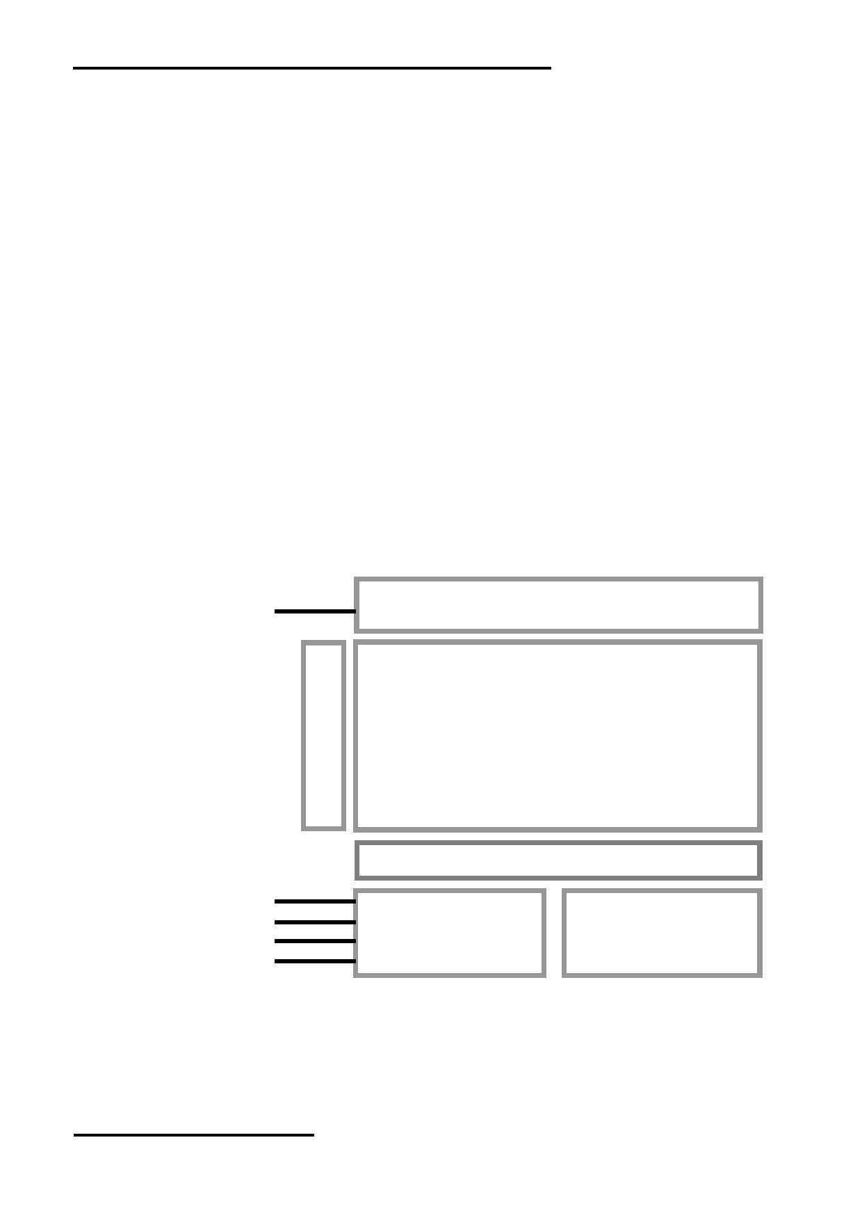
2. Block Diagram
BL_VDD, BL_GND
Backlight Circuit
BL_EN, BL_ADJ
800x 480 pixels
Source Driver
RX0+,RX0-,RX1+,RX1-
RX2+, RX2-
LVDS interface
Power Circuit
VCC_IN, GND
RXC+, RXC-
URL: www.topwaydisplay.com
Document Name: 错误 ! 未指定书签。 0.2
Page: 3 of 12
TOPWAY
LCD Module User Manual
LMT050DNCFWU-NBN
3. Terminal Function
3.1 K1 LVDS Terminal
Pin No.
Pin Name
IO
Descriptions
1
NC
2
NC
3
NC
-
No connection,leave open
4
NC
5
NC
6
RXC+
Input
LVDS receiver positive signal clock
7
NC
-
No connection
8
RXC-
Input
LVDS receiver negative signal clock
9
NC
-
No connection,leave open
10
RX2+
Input
LVDS receiver positive signal channel 2
11
NC
-
No connection,leave open
12
RX2-
Input
LVDS receiver negative signal channel 2
13
GND
Power Ground
14
RX1+
Input
LVDS receiver positive signal channel 1
15
GND
Power Ground
16
RX1-
Input
LVDS receiver negative signal channel 1
17
VCC_IN
Power Positive Power Supply(3.3V)
18
RX0+
Input
LVDS receiver positive signal channel 0
19
VCC_IN
Power Positive Power Supply(3.3V)
20
RX0-
Input
LVDS receiver negative signal channel 0
3.2 K2 Backlight Terminal
Pin No.
Pin Name
IO
Descriptions
1
BL_VDD
Power Positive Power Supply(5.0V)
Backlight Driver Control
2
BL_EN
Input
BL_EN=Hi, Backlight Driving Booster enable
BL_EN=Lo, Backlight Driving Booster disable
Backlight dimming control
3
BL_ADJ
Input
PWM may be used to adjust the output brightness
4
NC
-
No connection,leave open
5
NC
-
No connection,leave open
6
BL_GND
Power Power Supply GND (0V)
URL: www.topwaydisplay.com
Document Name: 错误 ! 未指定书签。 0.2
Page: 4 of 12
TOPWAY
LCD Module User Manual
LMT050DNCFWU-NBN
4. Absolute Maximum Ratings
Items
Symbol
Min.
Max.
Unit
Condition
Power Supply voltage
VCC_IN
-0.3
+3.6
V
Backlight Supply voltage
BL_VDD
-0.3
+6.0
V
Operating Temperature
T OP
-20
70
C
No Condensation
Storage Temperature
T ST
-30
80
C
No Condensation
Note:
*1. This rating applies to all parts of the module. And should not be exceeded.
*2. The operating temperature only guarantees operation of the circuit. The contrast, response speed,
and the other specification related to electro-optical display quality is determined at the room temperature, T OP =25 ℃
*3. Ambient temperature when the backlight is lit (reference value)
*4. Any Stresses exceeding the Absolute Maximum Ratings may cause substantial damage to the device. Functional
operation of this device at other conditions beyond those listed in the specification is not implied and prolonged
exposure to extreme conditions may affect device reliability.
5. Electrical Characteristics
5.1 Driving TFT LCD Panel
Top=25 ℃ , VCC_IN =3.3V ,GND=0V
Items
Symbol
MIN.
TYP.
MAX.
Unit
Note
Supply Voltage
VCC_IN
3.0
3.3
3.6
V
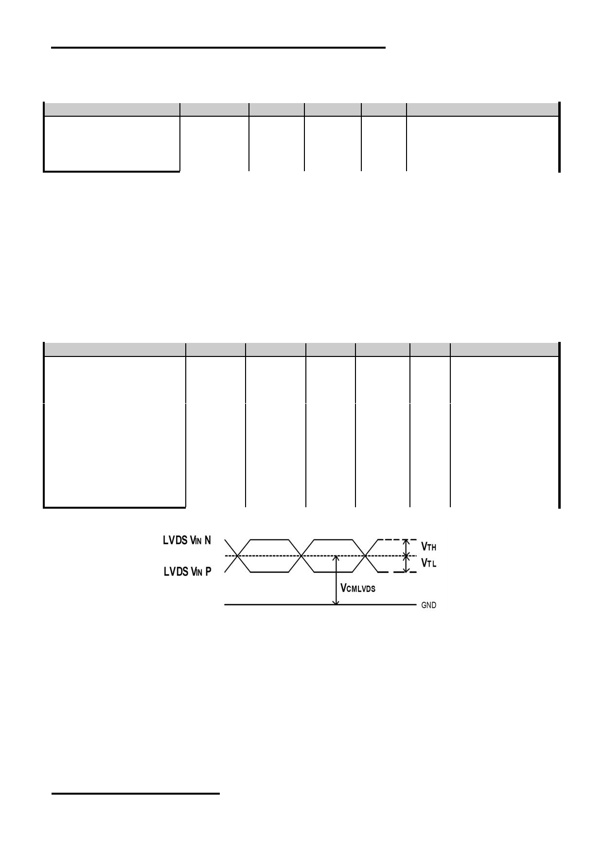
Common Electrode
V CMLVDS
V
Note1
Driving Signal
-
1.2
-
Differential Input High
V TH
-
-
100
mV
Threshold
Differential Input Low
V TL
-100
-
-
mV
Threshold
Sync Frequency
FVD
-
60
70
Hz
VDD Power Consumption
I VCC_IN
-
135
360
mA
LVDS DC timing diagram
Note1: The value may be different for different LCM.
URL: www.topwaydisplay.com
Document Name: 错误 ! 未指定书签。 0.2
Page: 5 of 12
TOPWAY
LCD Module User Manual
LMT050DNCFWU-NBN
5.2 LED Backlight Circuit Characteristics
BL_GND=0V, T OP =25 C
Parameter
Symbol
MIN.
TYP.
MAX.
Unit Note
Operating Voltage
V BL_VDD
4.7
5.0
5.3
V
Operating Current
I BL_VDD
-
190
-
mA
Note1
Input High Voltage
V IH
0.8V BL_VDD
-
V BL_VDD
V
BL_EN, BL_ADJ
Input Low Voltage
V IL
BL_GND
-
0.3
V
BL_EN, BL_ADJ
Cautions:
Exceeding the recommended driving current could cause substantial damage to the backlight and shorten its lifetime.
Note:
*1: BL_EN=Hi, BL_ADJ=Hi;
*2. Recommended BL_ADJ PWM Freq. is 3kHz .
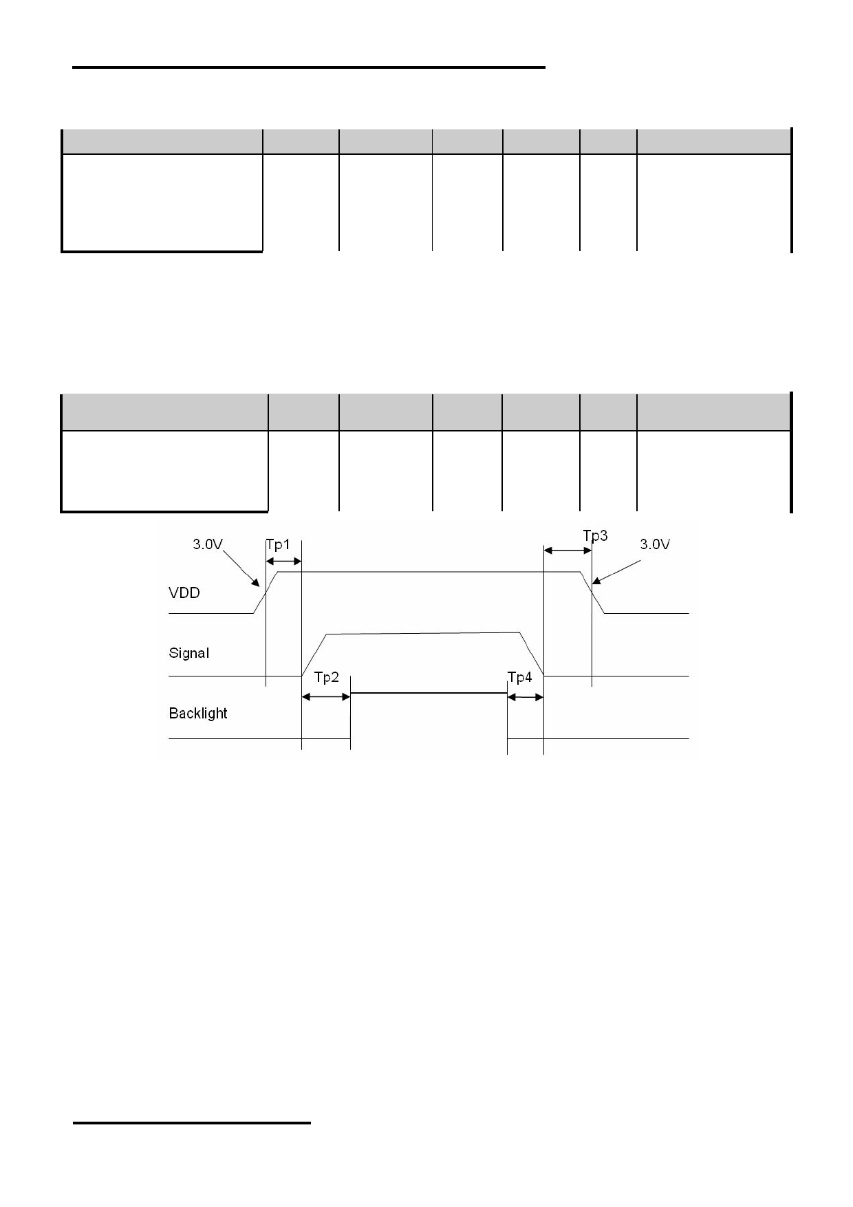
5.3 Power On/Off Sequence
Items
Symbo
MIN.
TYP.
Max.
Unit Note
l
VDD 3.0V to signal starting
Tp1
0
-
50
ms
Signal starting to backlight on
Tp2
150
-
-
ms
Signal off to VDD 3.0V
Tp3
0
-
50
ms
Backlight off to signal off
Tp4
150
-
-
ms
Interface Power On/Off Sequence
URL: www.topwaydisplay.com
Document Name: 错误 ! 未指定书签。 0.2
Page: 6 of 12
TOPWAY
LCD Module User Manual
LMT050DNCFWU-NBN
6. AC Characteristics
6.1 Timing Conditions
Item
Symbol
MIN.
TYP.
MAX.
Unit
Condition
Input CLK period
t RI CLK
8.9
-
50
ns
Input Data Position 0
( t RI CLK = 8.9ns )
t RI 0
-0.3
-
+0.3
ns
Input Data Position 1
t RI CLK/7-0.3
t RI CLK/7+0.3
(t RI CLK = 8.9ns )
t RI 1
t RI CLK/7
ns
Input Data Position 2
2t RI CLK/7-0.3
2t RI CLK/7
2t RI CLK/7+0.3
(t RI CLK = 8.9ns )
t RI 2
ns
Input Data Position 3
3t RI CLK/7
(t RI CLK = 8.9ns )
t RI 3
3t RI CLK/7-0.3
3t RI CLK/7+0.3
ns
Input Data Position 4
4t RI CLK/7
(t RI CLK = 8.9ns )
t RI 4
4t RI CLK/7-0.3
4t RI CLK/7+0.3
ns
Input Data Position 5
5t RI CLK/7
(t RI CLK = 8.9ns )
t RI 5
5t RI CLK/7-0.3
5t RI CLK/7+0.3
ns
Input Data Position 6
6t RI CLK/7
(t RI CLK = 8.9ns )
t RI 6
6t RI CLK/7-0.3
6t RI CLK/7+0.3
ns
URL: www.topwaydisplay.com
Document Name: 错误 ! 未指定书签。 0.2
Page: 7 of 12
TOPWAY
LCD Module User Manual
LMT050DNCFWU-NBN
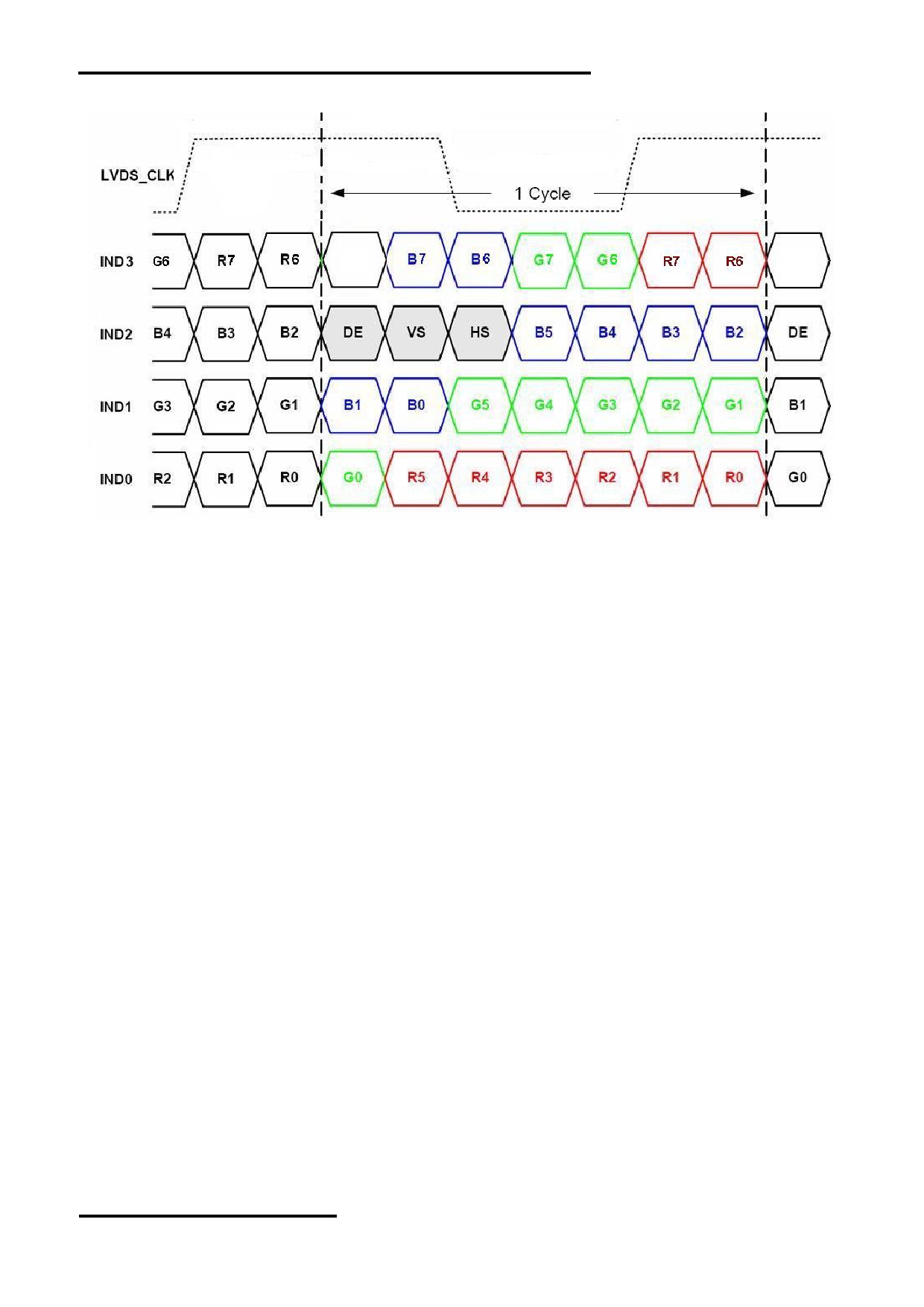
6.2 LVDS Timing Diagram
URL: www.topwaydisplay.com
Document Name: 错误 ! 未指定书签。 0.2
Page: 8 of 12
TOPWAY
LCD Module User Manual
LMT050DNCFWU-NBN
6.3 Data Input format
Item
Symbol
MIN.
TYP.
MAX.
Unit
Remark
Horizontal Display Area
thd
800
DCLK
CLKIN Frequency
fclk
-
30
50
MHz
One Horizontal Line
th
889
928
1143
CLKIN
HSD pulse width
thpw
1
48
255
CLKIN
HSD Blanking
thb
88
CLKIN
HSD Front Porch
thfp
1
40
255
CLKIN
Vertical Display Area
tvd
480
TH
VSD period time
tv
513
525
767
TH
VSD pulse width
tvpw
3
3
255
TH
VSD Blanking
tvb
32
TH
VSD Front Porch
tvfp
1
13
255
TH
Note:
1. LVDS signal should carry SYNC mode signals
Horizontal input timing diagram
Vertical input timing diagram
URL: www.topwaydisplay.com
Document Name: 错误 ! 未指定书签。 0.2
Page: 9 of 12
TOPWAY
LCD Module User Manual
LMT050DNCFWU-NBN
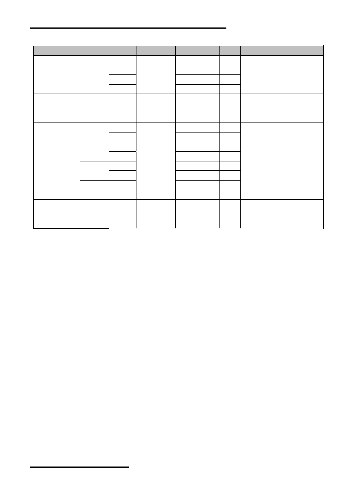
7. Optical Characteristics
Item
Symbol
Condition
MIN.
TYP.
MAX.
UNIT
Note.
θ T
40
50
-
Viewing angle
θ B
60
70
-
(CR ≥ 10)
degree
Note 2
θ L
60
70
-
θ R
60
70
-
Contrast ratio
CR
θ=0 o
500
600
-
-
Note 1,3
T on
msec
Response Time
25 ℃
-
20
30
Note 1,4
T off
msec
X
0.260 0.310 0.360
White
Y
0.280 0.330 0.380
X
0.540 0.590 0.640
Red
Y
Backlight
0.300 0.350 0.400
Chromaticlty
is on
Note 1,5
X
0.298 0.348 0.398
Green
Y
0.520 0.570 0.620
X
0.095 0.145 0.195
Blue
Y
0.060 0.110 0.160
Luminance
L
200
250
-
cd/m 2
Note 1,6
NTSC
-
50
%
Note 5
Luminance uniformity
U
75
80
-
%
Note 1,7
Test Conditions:
1. IF= 40mA, VF=21.7V, no touch panel, and the ambient temperature is 25 ℃ .
2. The test systems refer to Note 1 and Note 2.
URL: www.topwaydisplay.com
Document Name: 错误 ! 未指定书签。 0.2
Page: 10 of 12
TOPWAY
LCD Module User Manual
LMT050DNCFWU-NBN
Note 1:
Note 2:
The data are measured after LEDs are turned on for 5 minutes.
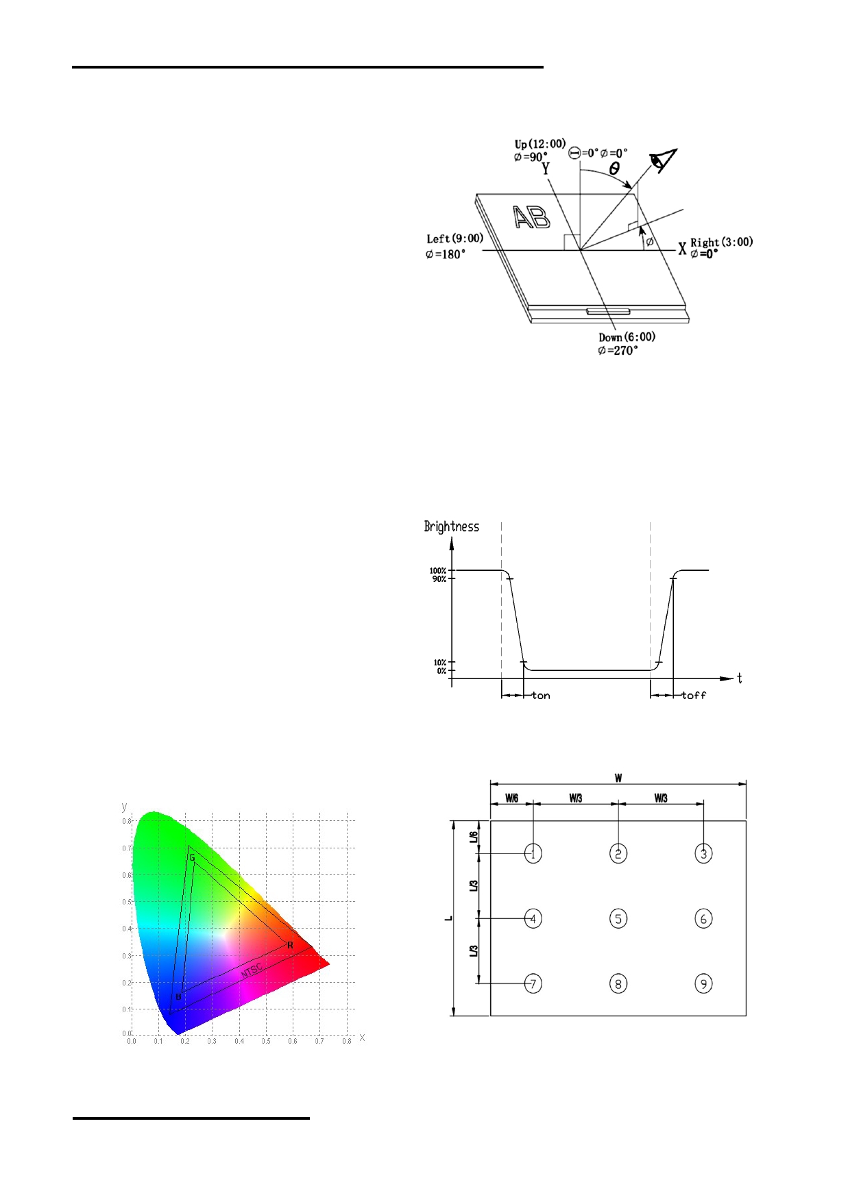
The definition of viewing angle:
LCM displays full white. The brightness is the average value of 9 Refer to the graph below marked by θ and Ф
measured spots. Measurement equipment SR-3A (1°)
Measuring condition:
- Measuring surroundings: Dark room
- Measuring temperature: Ta=25 ℃ .
- Adjust operating voltage to get optimum contrast at
the center of the display.
Note 3:
The definition of contrast ratio (Test LCM using SR-3A (1°)):
Note 4:
Contrast
Luminance When LCD is at “White” state
Definition of Response time. (Test LCD using BM-7A(2°)):
Ratio(CR)
=
Luminance When LCD is at “Black” state
The output signals of photo detector are measured
(Contrast Ratio is measured in optimum common electrode
when the input signals are changed from
voltage)
“black” to “white”(falling time)
and from “white” to “black”(rising time), respectively.
The response time is defined as
the time interval between the 10% and 90% of amplitudes.Refer to
figure as below.
Note 5:
Note 6:
Definition of Color of CIE1931 Coordinate and NTSC Ratio.
The luminance uniformity is calculated by using following formula.
△ Bp = Bp (Min.) / Bp (Max.)×100 (%)
Color gamut:
Bp (Max.) = Maximum brightness in 9 measured spots
Area of RGB triangle
S=
X100%
Bp (Min.) = Minimum brightness in 9 measured spots .
Area of NTSC triangle
Note 7:
Measured the luminance of white state at center point
URL: www.topwaydisplay.com
Document Name: 错误 ! 未指定书签。 0.2
Page: 11 of 12

TOPWAY
LCD Module User Manual
LMT050DNCFWU-NBN
8. Precautions of using LCD Modules
Please refer to "LCD-Module-Design-Handling-Precaution.pdf".
URL: www.topwaydisplay.com
Document Name: 错误 ! 未指定书签。 0.2
Page: 12 of 12