LMT070DICFWD-NSD-1
LCD Module User Manual
Prepared by:
Checked by:
Approved by:
Yu
Date: 2019-08-21
Date:
Date:
Rev. Descriptions
Release Date
0.1
Preliminary release
2019-08-21
URL: www.topwaydisplay.com
Document Name:LMT070DICFWD-NSD-1-Manual-Rev0.1
Page: 1 of 19

TOPWAY
LCD Module User Manual
LMT070DICFWD-NSD-1
Table of Content
1. General Specification ............................................................................................................ 3
2. Block Diagram ........................................................................................................................ 3
3. Terminal Function (Input Terminal) ...................................................................................... 4
4. Absolute Maximum Ratings .................................................................................................. 4
5. Electrical Characteristics ...................................................................................................... 5
5.1
DC Characteristics ................................................................................................................................................. 5
5.2
Power Sequence .................................................................................................................................................... 5
6. AC Characteristics ................................................................................................................. 6
6.1
Timing Characteristics ............................................................................................................................................ 6
6.2
Input Clock and Data Timing Diagram ................................................................................................................... 6
6.3
AC Timing .............................................................................................................................................................. 7
6.4
Data Input Format .................................................................................................................................................. 7
7. CTP Function Characteristics ............................................................................................... 8
7.1
I 2 C Communication ................................................................................................................................................ 8
7.2
Data Transmission ................................................................................................................................................. 9
7.3
Register Information of CTP ................................................................................................................................. 10
8. Optical Characteristics ........................................................................................................ 17
9. Precautions of using LCD Modules .................................................................................... 18
URL: www.topwaydisplay.com
Document Name:LMT070DICFWD-NSD-1-Manual-Rev0.1
Page: 2 of 19
TOPWAY
LCD Module User Manual
LMT070DICFWD-NSD-1
General Specification
Signal Interface :
Digital 24-bits RGB
Display Technology :
a-Si TFT active matrix
Display Mode :
TN Type Full Color / Transmissive / Normal White
Screen Size(Diagonal) :
7.0”
Outline Dimension :
164.9 x 100.0 x 10.88 MAX (mm)
(see attached drawing for details)
Active Area :
154.08 x 85.92 (mm)
Number of dots :
800 x 480
Pixel Pitch :
0.1926 x 0.179 (mm)
Pixel Configuration :
RGB Stripe
Backlight :
LED
Viewing Direction :
12 o’clock(Gray scale Inversion) (*1)
6 o’clock (*2)
Touch Panel Type:
Capacitive Touch Panel
Operating Temperature :
-20 ~ +70°C
Storage Temperature :
-30 ~ +80°C
Note:
*1. For saturated color display content (eg. pure-red, pure-green, pure-blue or pure-colors-combinations).
*2. For “ color scales ” display content.
*3. Color tone may slightly change by temperature and driving condition.
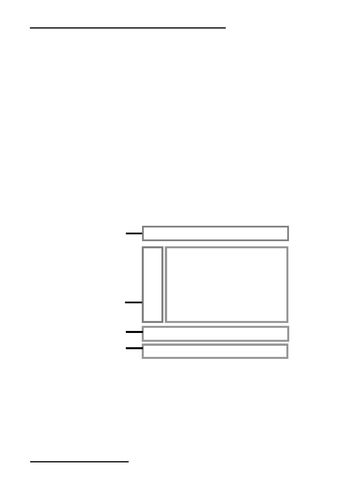
Block Diagram
/TPRST, /TPINT
TPSDA, TPSCL
Capacitive Touch Panel
R0~R7, G0~G7,B0~B7,
7’’ TFT Panel
DCLK, DE, HS,VS, MODE
BLADJ, BLEN
Backlight Circuit
+5V, GND
Power Circuit
URL: www.topwaydisplay.com
Document Name:LMT070DICFWD-NSD-1-Manual-Rev0.1
Page: 3 of 19
TOPWAY
LCD Module User Manual
LMT070DICFWD-NSD-1
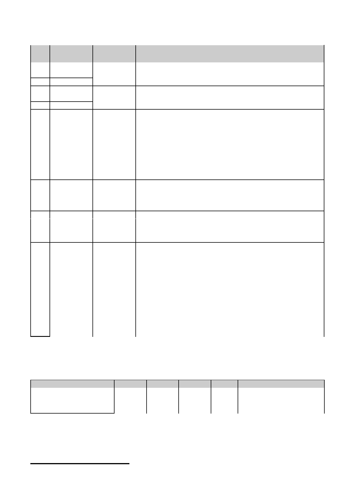
Terminal Function (Input Terminal)
Pin Pin
No. Name
I/O
Descriptions
1
5V
:
:
Power
5V power supply
5
5V
6
GND
:
:
Power
0V power supply
10
GND
11
BLADJ
Input
Backlight brightness PWM signal (active low)
12
BLEN
Input
Backlight enable signal (active high)
13
MODE
Input
when MODE = “1”: DE mode (default).
when MODE = “0”: SYNC mode, DE must be grounded.
14
DE
Input
Data Input Enable
15
VS
Input
Vertical sync signal
16
HS
Input
Horizontal sync signal
17
B7
:
:
Input
Blue data line
23
B1
Input
Blue data line(*1)
24
B0
Input
Blue data line(*1)
25
G7
:
:
Input
Green data line
31
G1
Input
Green data line(*1)
32
G0
Input
Green data line(*1)
33
R7
:
:
Input
Red data line
39
R1
Input
Red data line(*1)
40
R0
Input
Red data line(*1)
41
GND
Power
Ground, 0V
42
DCLK
Input
Pixel clock(*2)
43
GND
Power
Ground, 0V
44
NC
NC
No Connection
45
GND
Power
Ground, 0V
46
/TPRST
Input
Reset signal, active low reset
47
/TPINT
Output
Interrupt signal, active low interrupt
48
TPSDA
I/O
I2C data (*3)
49
TPSCL
Input
I2C clock (*3)
50
GND
Power
Ground
Note:
*1. When input 18bits RGB data, the two low bits of R,G and B data must be grounded.
*2. Data shall be latched at the falling edge of DCLK.
*3. With internal resister(4.7k) pull up.
Absolute Maximum Ratings
Items
Symbol
Min.
Max.
Unit
Condition
Power Voltage
V 5V
-0.3
+5.5
V
GND = 0V
Operating Temperature
T OP
-20
+70
℃
No Condensation
Storage Temperature
T ST
-30
+80
℃
No Condensation
Cautions:
Any Stresses exceeding the Absolute Maximum Ratings may cause substantial damage to the device. Functional
operation of this device at other conditions beyond those listed in the specification is not implied and prolonged exposure
to extreme conditions may affect device reliability.
URL: www.topwaydisplay.com
Document Name:LMT070DICFWD-NSD-1-Manual-Rev0.1
Page: 4 of 19
TOPWAY
LCD Module User Manual
LMT070DICFWD-NSD-1
Electrical Characteristics
DC Characteristics
GND=0V, V 5V =5.0V, T OP =25 ℃
Items
Symbol
MIN.
TYP.
MAX.
Unit Applicable Pin
Power Voltage
V 5V
4.5
5.0
5.5
V
5V
Operating Current (*1)
I 5V
-
510
1020
mA
Input High Voltage
V IH
3.0
-
3.6
V
Input pins
Input Low Voltage
V IL
0
-
0.3
V
Input pins
Output Signal High Voltage
V oH
3.0
-
3.6
V
Output Signal Low Voltage
V oL
0
-
0.6
V
Note:
*1. For different LCM, the value may have a bit of difference.
*2. To test the current dissipation, use “all Black Pattern”.
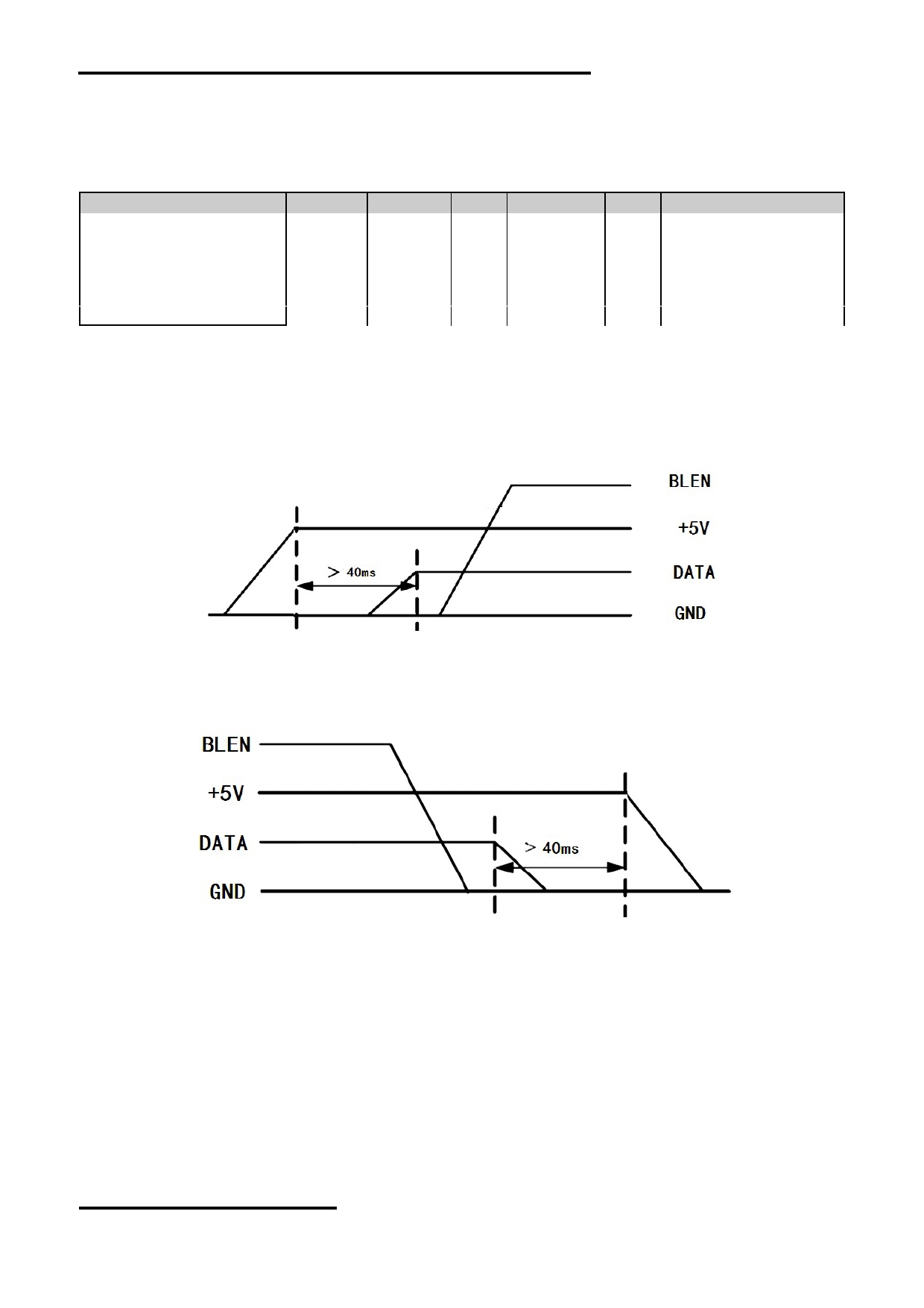
Power Sequence
Power on:
+5V → DATA → BLEN
Power off:
BLEN → DATA → +5V
Note :Data include R0~R7,B0~B7,G0~G7, DCLK, HS, VS, DE, MODE, /TPRST, /TPINT, TPSDA, TPSCL.
URL: www.topwaydisplay.com
Document Name:LMT070DICFWD-NSD-1-Manual-Rev0.1
Page: 5 of 19
TOPWAY
LCD Module User Manual
LMT070DICFWD-NSD-1
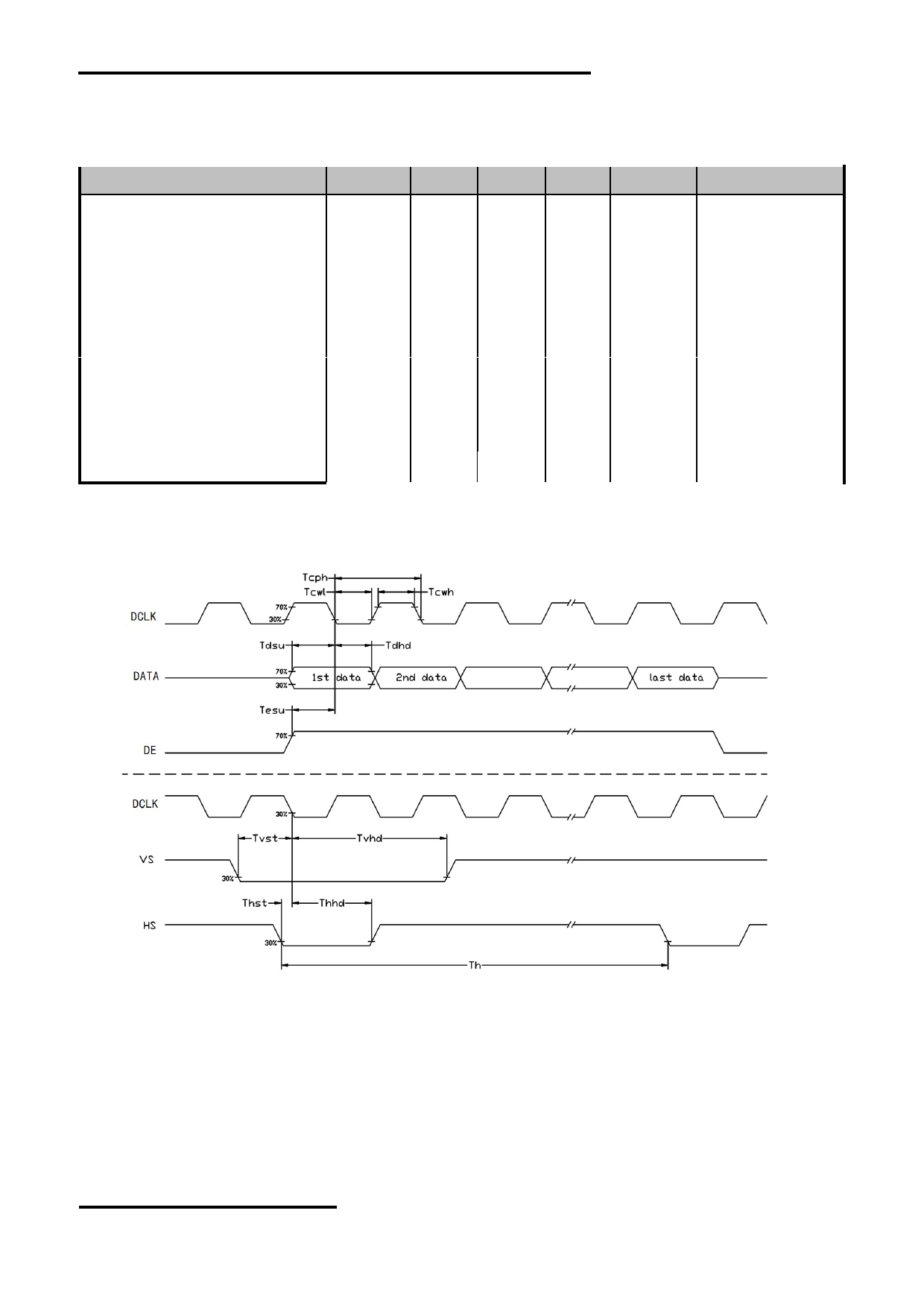
AC Characteristics
Timing Characteristics
Item
Symbol
MIN.
TYP.
MAX.
Unit
Remark
HS setup time
Thst
8
-
-
ns
HS hold time
Thhd
8
-
-
ns
VS setup time
Tvst
8
-
-
ns
VS hold time
Tvhd
8
-
-
ns
Data setup time
Tdsu
8
-
-
ns
Data hole time
Tdhd
8
-
-
ns
DE setup time
Tesu
8
-
-
ns
DV DD Power On Slew rate
TPOR
-
-
20
ms
From 0 to 90%
DV DD
DCLK cycle time
Tcph
20
-
-
ns
DCLK pulse duty
Tcwh
40
50
60
%
Note: For the details of the timing, please see the Driver IC data sheet.
Input Clock and Data Timing Diagram
URL: www.topwaydisplay.com
Document Name:LMT070DICFWD-NSD-1-Manual-Rev0.1
Page: 6 of 19
TOPWAY
LCD Module User Manual
LMT070DICFWD-NSD-1
AC Timing
Item
Symbol
MIN.
TYP.
MAX. Unit
Remark
Horizontal Display Area
thd
-
800
-
DCLK
DCLK Frequency
fclk
26.4
33.3
46.8
MHz
One Horizontal Line
th
862
1056
1200
DCLK
HS pulse width
thpw
1
-
40
DCLK
HS Blanking
thb
46
46
46
DCLK
HS Front Porch
thfp
16
210
354
DCLK
Vertical Display Area
tvd
-
480
-
TH
VS period time
tv
510
525
650
TH
VS pulse width
tvpw
1
-
20
TH
VS Blanking
tvb
23
23
23
TH
VS Front Porch
tvfp
7
22
147
TH
Data Input Format
Horizontal input timing diagram.
Vertical input timing diagram.
URL: www.topwaydisplay.com
Document Name:LMT070DICFWD-NSD-1-Manual-Rev0.1
Page: 7 of 19
TOPWAY
LCD Module User Manual
LMT070DICFWD-NSD-1
CTP Function Characteristics
I 2 C Communication
CTP provides standard I 2 C interface for communication. In the system, CTP always works in slave
mode, all communications are initiated by master, and the baud rate can be up to 400Kbps. The
definition of I 2 C timing is as following:
Parameter
Symbol
Min.
Max.
Unit
SCL low period
t lo
1.3
-
us
SCL high period
t hi
0.6
-
us
SCL setup time for start condition
t st1
0.6
-
us
SCL setup time for stop condition
t st3
0.6
-
us
SCL hold time for start condition
t hd1
0.6
-
us
SDA setup time
t st2
0.1
-
us
SDA hold time
t hd2
0
-
us
I 2 C Timing
CTP has 2 sets of slave address 0xBA/0xBB & 0x28/29. Master can control Reset & INT pin to
configure the slave address in power on initial state like following:
Power on diagram:
Timing of setting slave address to 0x28/0x29:
URL: www.topwaydisplay.com
Document Name:LMT070DICFWD-NSD-1-Manual-Rev0.1
Page: 8 of 19
TOPWAY
LCD Module User Manual
LMT070DICFWD-NSD-1
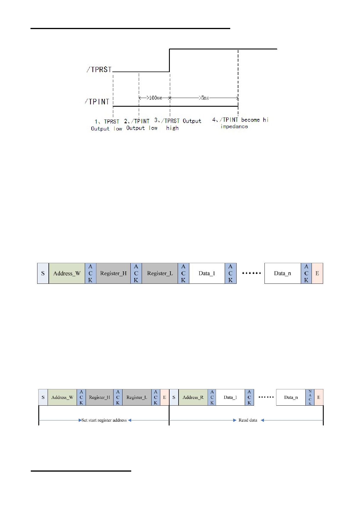
Timing of setting slave address to 0xBA/0xBB:
Data Transmission
(ex: slave address is 0xBA/0xBB)
Communication is always initiated by master, A high-to-low transition of SDA with SCL high is a start
condition.
All addressing signal are serially transmitted to and from on bus in 8-bit word. CTP sends a“0” to
acknowledge when the addressing word is 0xBA/BB (or 0x28/0x29 ). This happens during the ninth
clock cycle. If the slave address is not matched, CTP will stay in idle state.
The data words are serially transmitted to and from in 9-bit formation: 8-bit data + 1-bit ACK or NACK
sent by CTP. Data changes during SCL low periods & keeps valid during SCL high.
A low-to-high transition of SDA with SCL high is a stop condition.
Write Data to CTP
Write Operations
Please check the above figure, master start the communication first, and then sends device address
0XBA preparing for a write operation.
After receiving ACK from CTP, master sends out 16-bit register address, and then the data word in 8-bit,
which is going to be wrote into CTP.
The address pointer of CTP will automatically increase one after one byte writing, so master can
sequentially write in one operation. When operation finished, master stop the communication.
Read Data from CTP
(ex: slave address is 0xBA/0xBB)
Read Operations
Please check the above figure, master start the communication first, and then sends device address
0xBA for a write operation.
After receiving ACK from CTP, master sends out 16-bit register address, to set the address pointer of
URL: www.topwaydisplay.com
Document Name:LMT070DICFWD-NSD-1-Manual-Rev0.1
Page: 9 of 19
TOPWAY
LCD Module User Manual
LMT070DICFWD-NSD-1
CTP. After receiving ACK, master produce start signal once again & send device address 0xBB , then
read data word from CTP in 8-bit.
CTP also supports sequential read operation, and the default setting is sequential read mode.
Master shall send out ACK after every byte reading successfully but NACK after the last one.
Then sends stop signal to finish the communication.
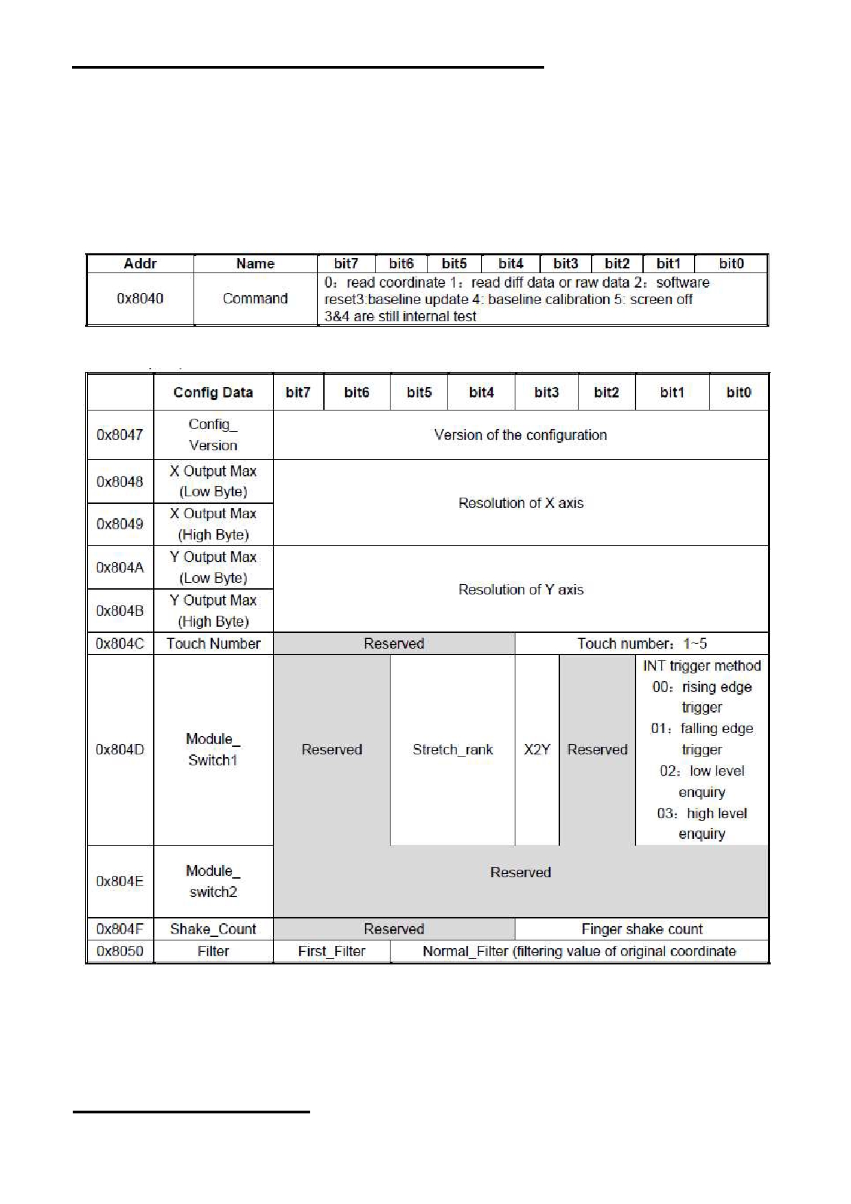
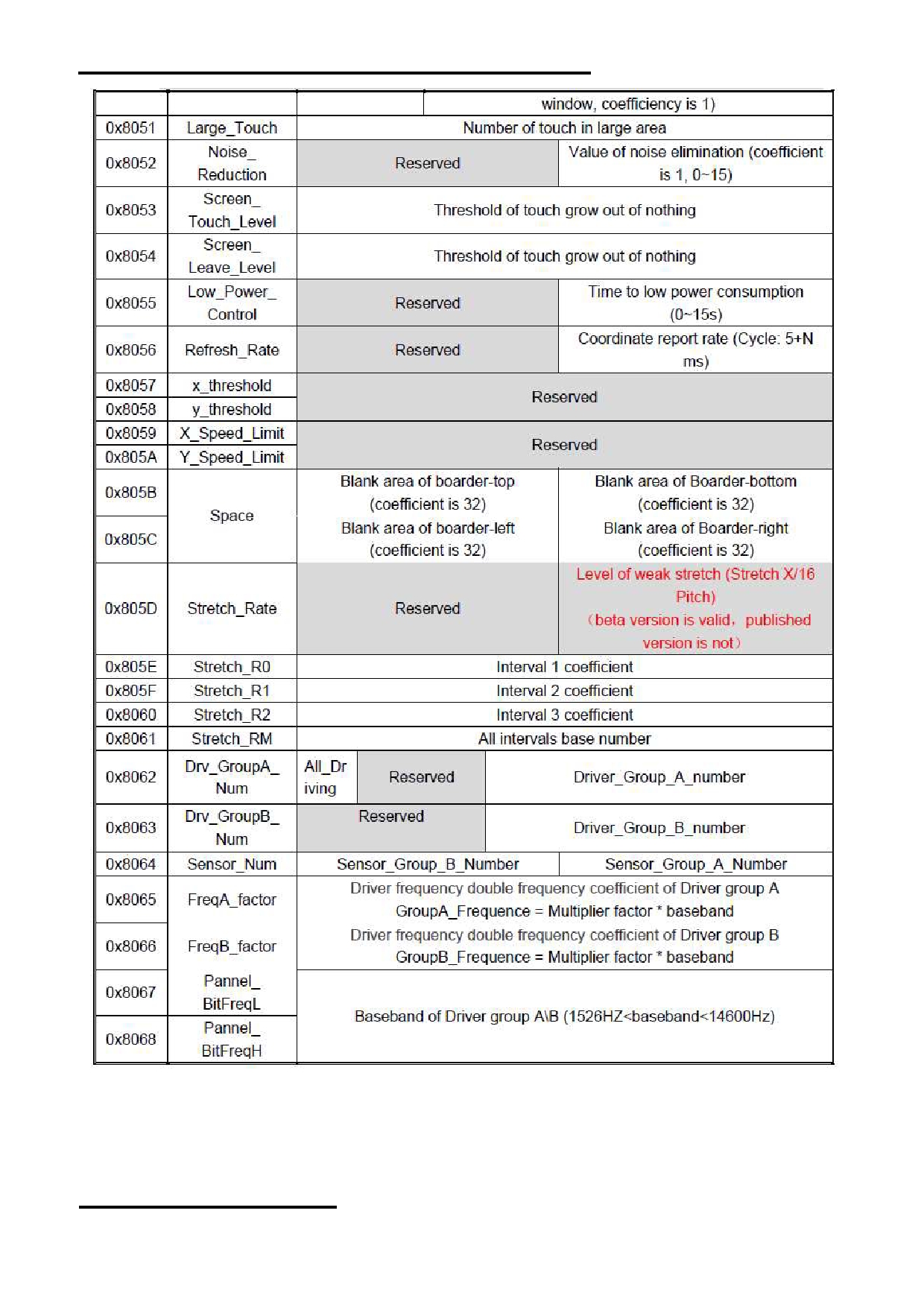
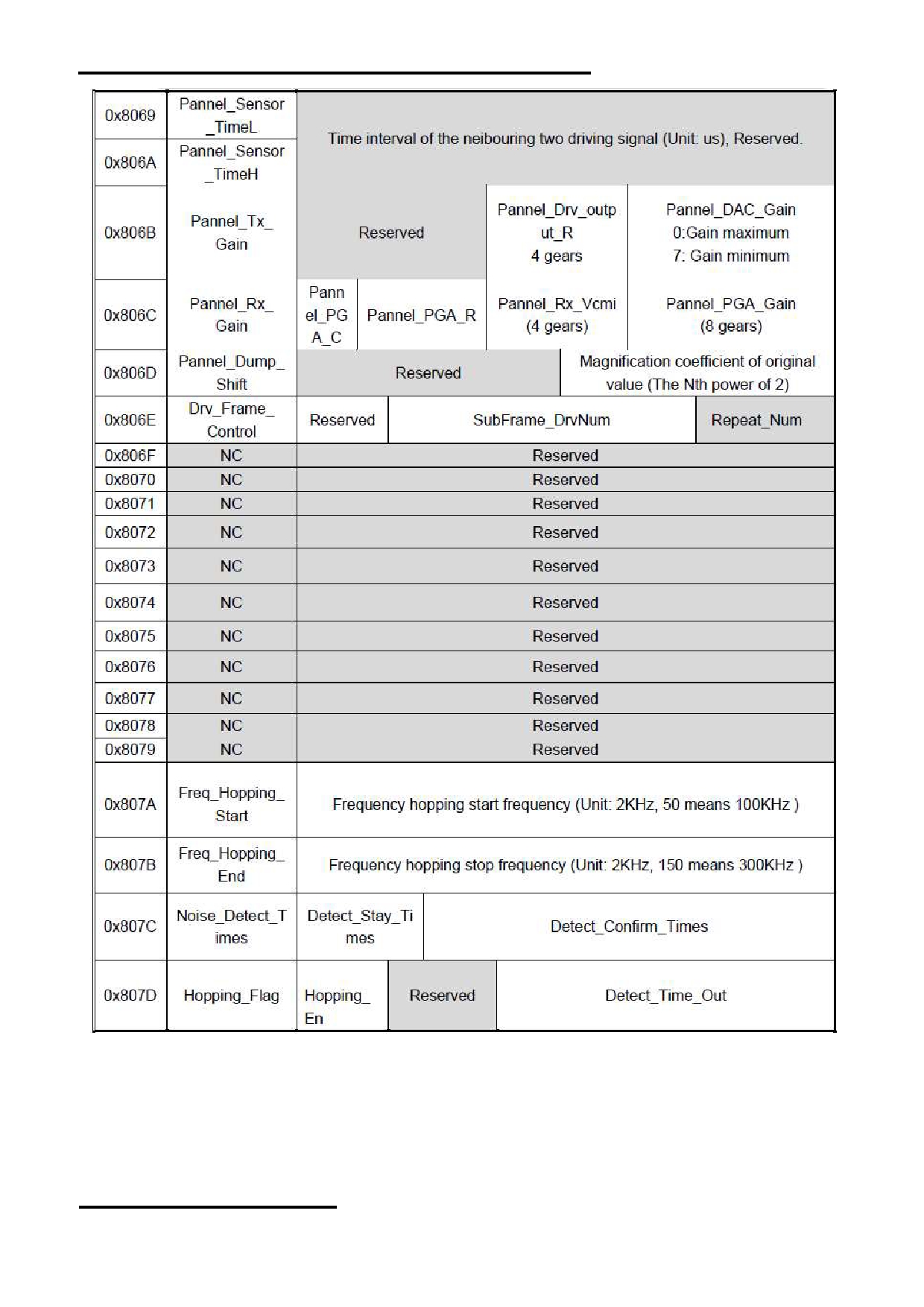
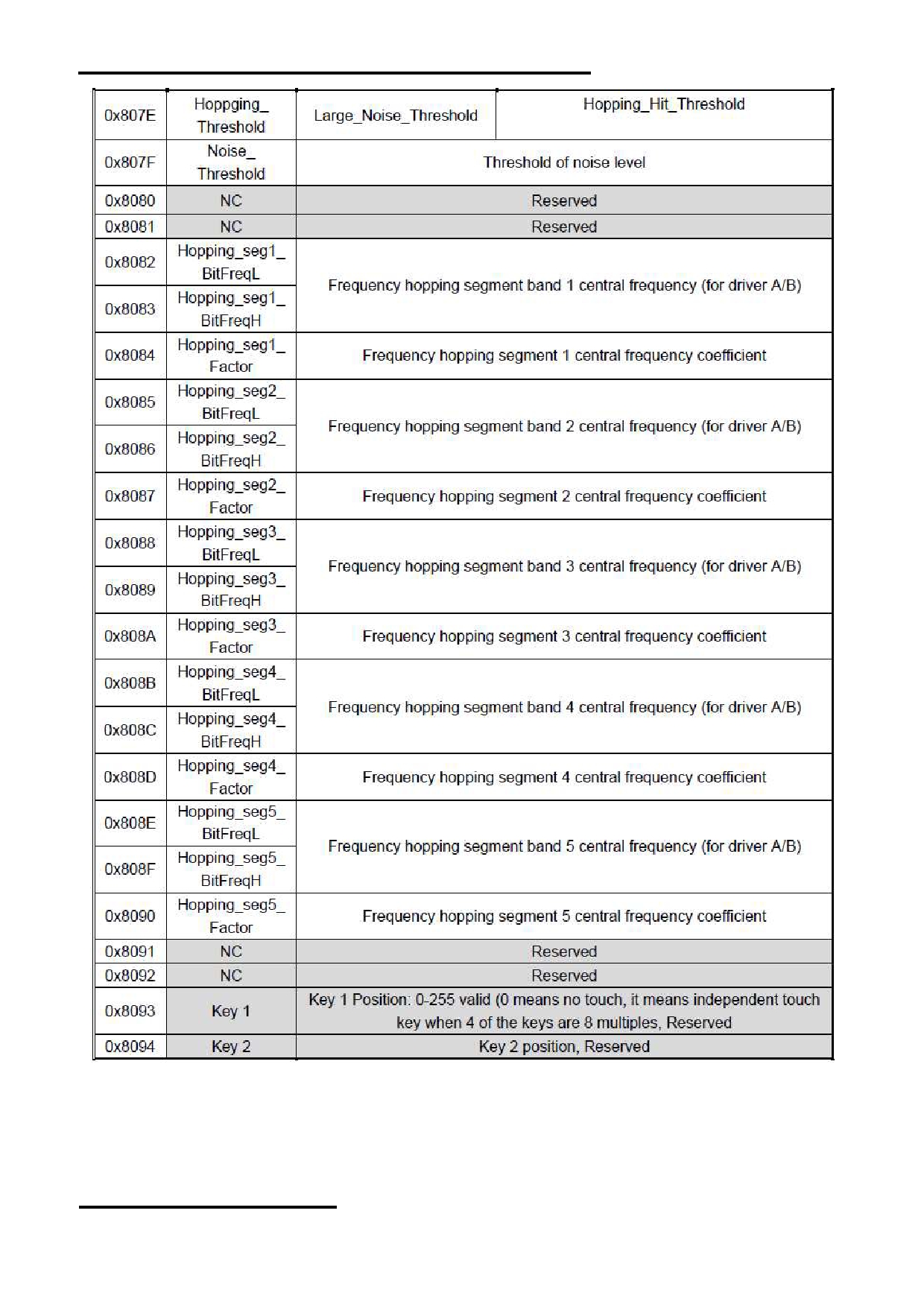
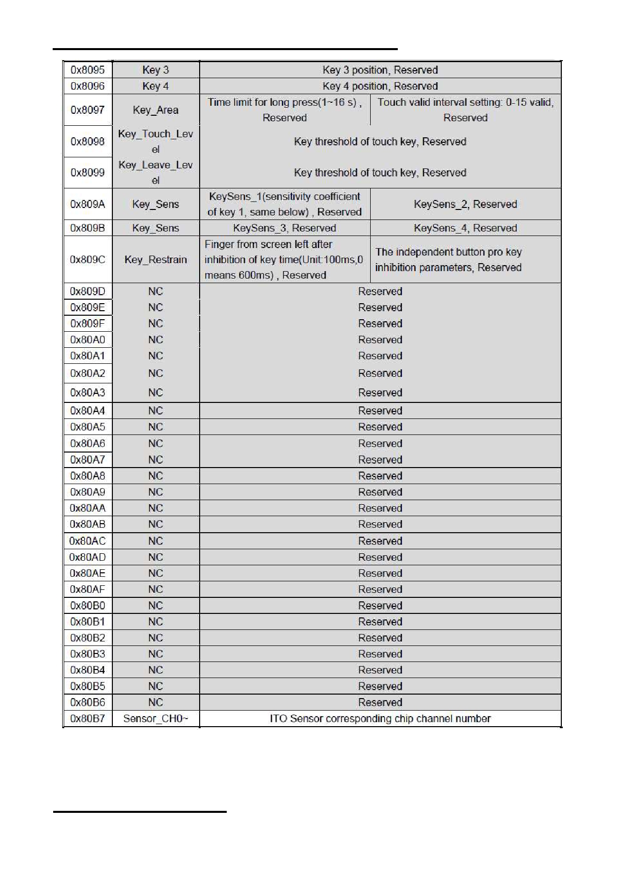
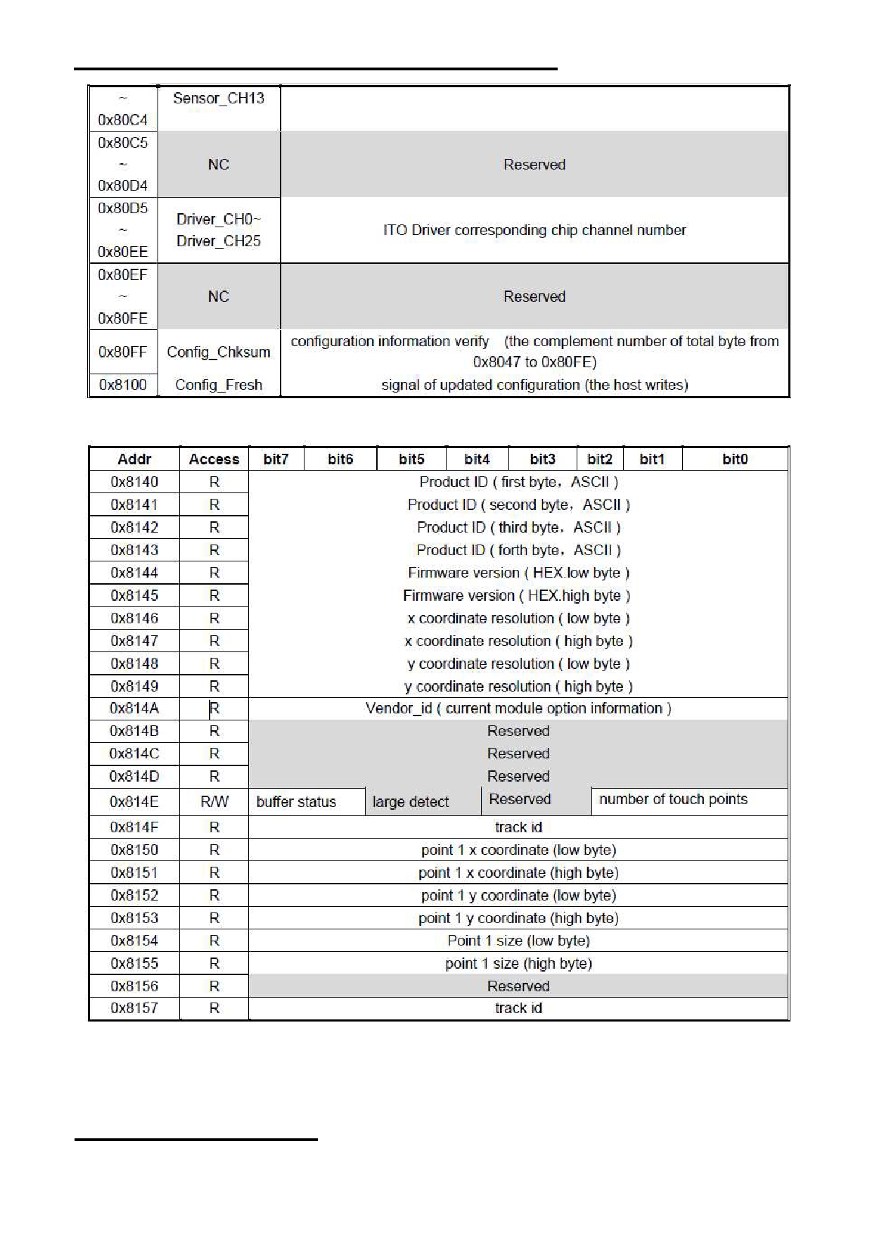
Register Information of CTP
Real Time Order(Write Only)
Configuration Information(R/W)
URL: www.topwaydisplay.com
Document Name:LMT070DICFWD-NSD-1-Manual-Rev0.1
Page: 10 of 19
TOPWAY
LCD Module User Manual
LMT070DICFWD-NSD-1
URL: www.topwaydisplay.com
Document Name:LMT070DICFWD-NSD-1-Manual-Rev0.1
Page: 11 of 19
TOPWAY
LCD Module User Manual
LMT070DICFWD-NSD-1
URL: www.topwaydisplay.com
Document Name:LMT070DICFWD-NSD-1-Manual-Rev0.1
Page: 12 of 19
TOPWAY
LCD Module User Manual
LMT070DICFWD-NSD-1
URL: www.topwaydisplay.com
Document Name:LMT070DICFWD-NSD-1-Manual-Rev0.1
Page: 13 of 19
TOPWAY
LCD Module User Manual
LMT070DICFWD-NSD-1
URL: www.topwaydisplay.com
Document Name:LMT070DICFWD-NSD-1-Manual-Rev0.1
Page: 14 of 19
TOPWAY
LCD Module User Manual
LMT070DICFWD-NSD-1
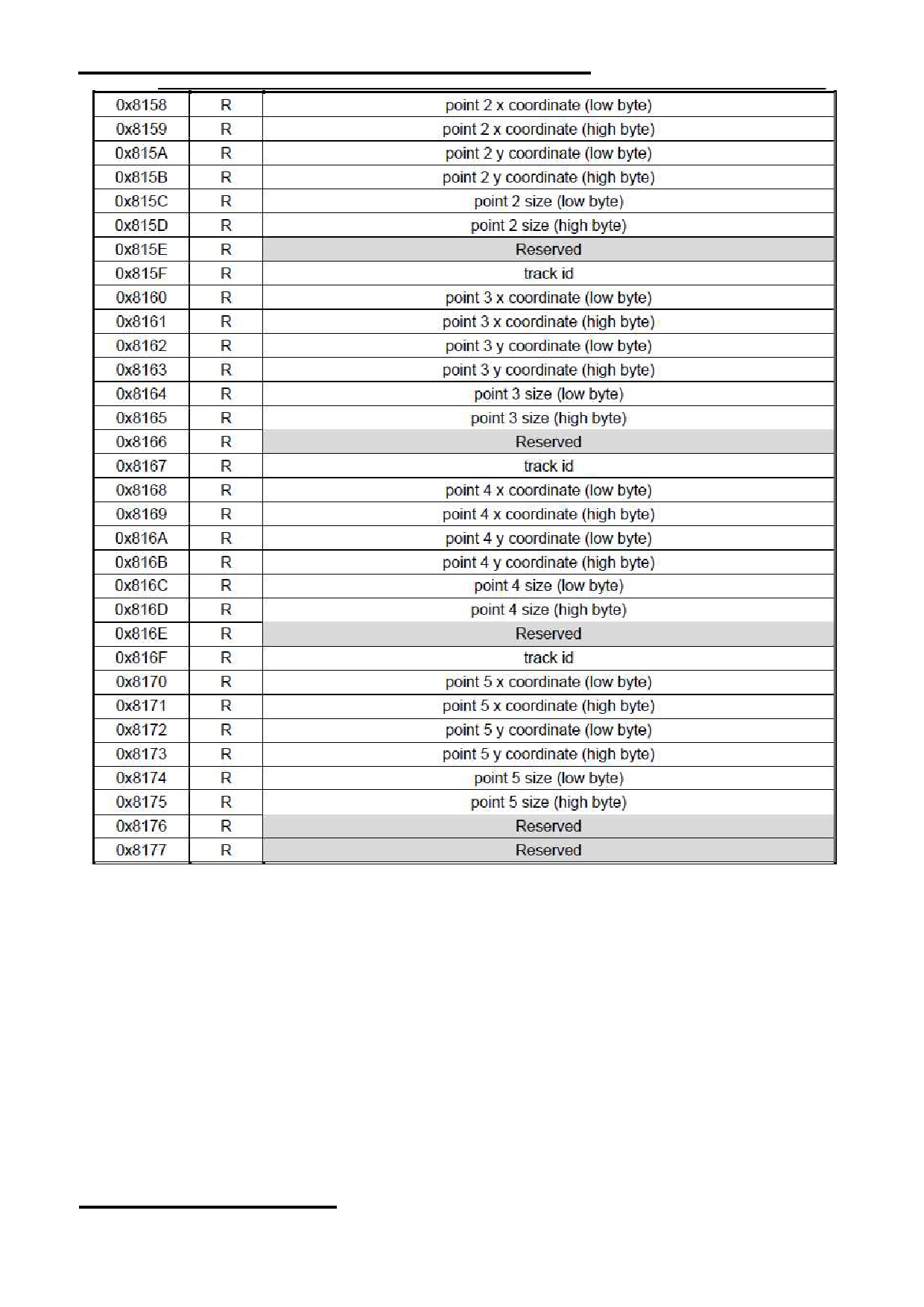
Coordinates Information
URL: www.topwaydisplay.com
Document Name:LMT070DICFWD-NSD-1-Manual-Rev0.1
Page: 15 of 19
TOPWAY
LCD Module User Manual
LMT070DICFWD-NSD-1
Note:
Please refer to GT911 IC datasheet for details.
URL: www.topwaydisplay.com
Document Name:LMT070DICFWD-NSD-1-Manual-Rev0.1
Page: 16 of 19
TOPWAY
LCD Module User Manual
LMT070DICFWD-NSD-1
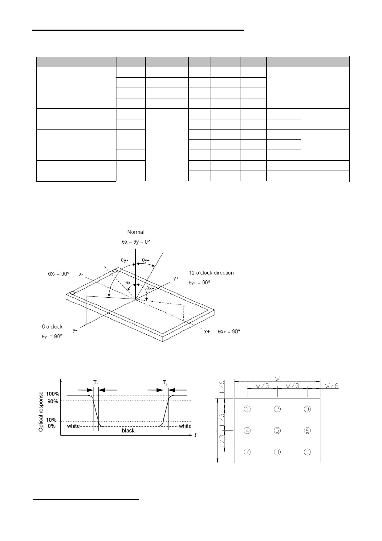
Optical Characteristics
Item
Symbol
Condition
MIN.
TYP.
MAX.
UNIT
Note.
θ R
3 o’clock
60
70
-
Viewing angle
θ L
9 o’clock
60
70
-
(CR ≥ 10)
degree
*2
θ B
6 o’clock
40
50
-
θ T
12 o’clock
60
70
-
T f
-
10
20
msec
Response Time
*3
T r
-
15
30
msec
Contrast ratio
CR
400
500
-
-
Normal
W X
0.26
0.31
0.26
-
*1
Color chromaticity
θ=0 o
W Y
0.28
0.33
0.38
-
Luminance
L
-
400
-
cd/m 2
*4
Luminance uniformity
Y U
70
75
-
%
*4
Note:
*1. Definition of Contrast Ratio
The contrast ratio could be calculate by the following expression:
Contrast Ratio (CR) = Luminance with all pixels white / Luminance with all pixels black
*2 Definition of Viewing Angle
*4 Definition of Luminance Uniformity
Luminance uniformity (Lu)=
*3 Definition of response time
Min. Luminance form pt1~pt9 / Max Luminance form Pt1~pt9
URL: www.topwaydisplay.com
Document Name:LMT070DICFWD-NSD-1-Manual-Rev0.1
Page: 17 of 19
TOPWAY
LCD Module User Manual
LMT070DICFWD-NSD-1
Precautions of using LCD Modules
Please refer to "LCD-Module-Design-Handling-Precaution.pdf".
附录一:
CTP Application Precautions
1. CTP Mounting Precaution
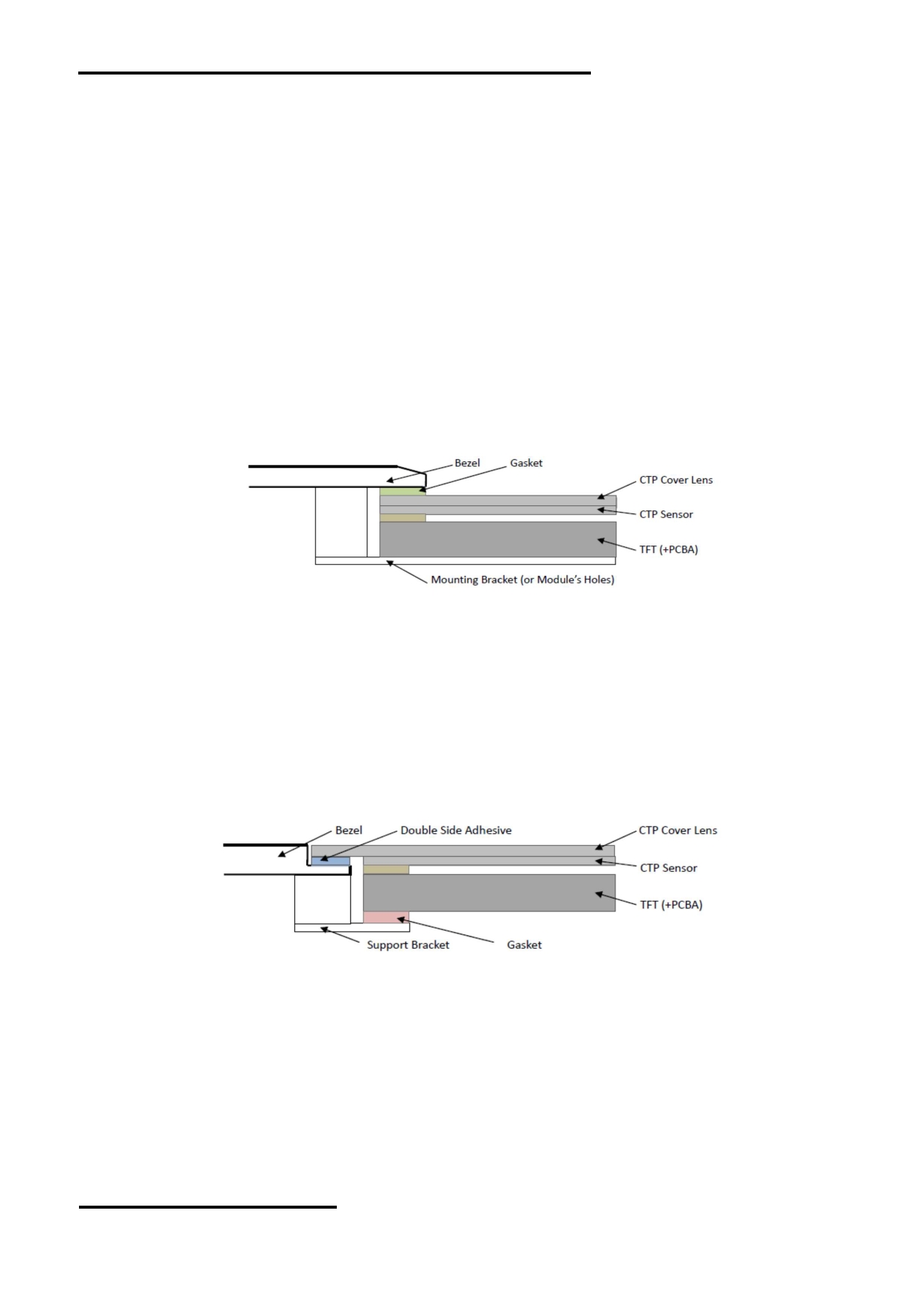
1.1 Bezel Mounting (Figure 1)
- The bezel window should be bigger than the CTP active area. It should be ≥ 0.5mm each side.
- Gasket should be installed between the bezel and the CTP surface.
The final gap should be about 0.5~1.0mm.
- It is recommended to provide an additional support bracket for backside support when
necessary (e.g. slim type TFT module without mounding structure). They should only provide
appropriate support and keep the module in place.
- The mounting structure should be strong enough to prevent external uneven force or twist act
onto the module.
Figure 1
1.2 Surface Mounting (Figure 2)
- As the CTP assembling on the countersink area with double side adhesive.
The countersink area should be flat and clean to ensure the double side adhesive installation
result.
- The Bezel is recommend to keep a gap ( ≥ 0.3mm each side) around the cover lens for
tolerance.
- It is recommended to provide an additional support bracket with gasket for backside support
when necessary (e.g. TFT module without mounding structure). They should only provide
appropriate support and keep the module in place.
- The mounting structure should be strong enough to prevent external uneven force or twist act
onto the module.
Figure 2
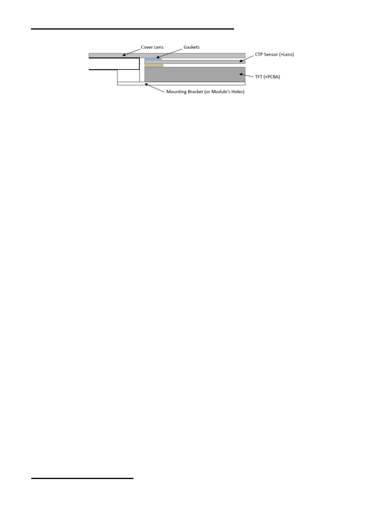
1.3 Additional Cover Lens Mounting (Figure 3)
- For the case of additional cover Lens mounting, it is necessary to recheck with the CTP
specification about the material and thickness to ensure the functionality.
- It should keep a 0.2~0.3mm gap between the cover lens and the CTP surface..
- The cover lens window should be bigger than the active area of the CTP.
It should be ≥ 0.5mm each side.
- It is recommended to provide an additional support bracket for backside support when
necessary (e.g. slim type TFT module without mounding structure). They should only provide
appropriate support and keep the module in place.
- The mounting structure should be strong enough to prevent external uneven force or twist act
onto the module.
URL: www.topwaydisplay.com
Document Name:LMT070DICFWD-NSD-1-Manual-Rev0.1
Page: 18 of 19
TOPWAY
LCD Module User Manual
LMT070DICFWD-NSD-1
Figure 3
2. Handling Precautions
2.1 The product made of glass. Do not subject it to a mechanical shock by dropping it from a high
place, etc.
2.2 Do not apply excessive or uneven force to the product since this may damage to the
performance.
2.3 If the display surface is contaminated, breathe on the surface and gently wipe it with a soft dry
cloth. If still not completely clear, moisten cloth with Isopropyl alcohol or Ethyl alcohol solvents.
Solvents other than those mentioned above may damage the product. Especially, do not use
Water, Ketone, Aromatic solvents.
2.4 Do not attempt to disassemble the CTP Module.
2.5 If the logic circuit power is off, do not apply the input signals.
2.6 To prevent destruction of the elements by static electricity, be careful to maintain an optimum
work environment.
a. Be sure to ground the body when handling the CTP Modules.
b. Tools required for assembly, such as soldering irons, must be properly ground.
c. To reduce the amount of static electricity generated, do not conduct assembly and other work
under dry conditions.
d. The CTP Module is coated with a film to protect the display surface. Be care when peeling off
this protective film since static electricity may be generated.
3. Storage and Transportation Precautions
3.1 When storing the CTP modules, avoid exposure to direct sunlight or to the light of fluorescent
lamps.
3.2 The CTP modules should be stored the required temperature range. If the CTP modules will be
stored for a long time, the recommend condition is the temperature of 0~40 ℃ and relative
humidity of ≤ 80%.
3.3 The LCD modules should be stored in the room without acid, alkali and harmful gas.
3.4 The CTP modules should be no falling and violent shocking during transportation, and also
should avoid excessive press, water, damp and sunshine.
URL: www.topwaydisplay.com
Document Name:LMT070DICFWD-NSD-1-Manual-Rev0.1
Page: 19 of 19