LMT070DNCFWD-NNA
LCD Module User Manual
Prepared by:
Checked by:
Approved by:
Huchubin
Date: 2020-12-12
Date:
Date:
Rev.
Descriptions
Edit
Release Date
0.1
Preliminary release
Huchubin
2020-12-12
Document Name: LMT070DNCFWD-NNA-Manual-Rev0.1.DOC
Page: 1 of 15

TOPWAY
LCD Module User Manual
LMT070DNCFWD-NNA
Table of Content
1.
Applications................................................................................................ ........................... 3
2. General Specification ................................................................................................ ............ 3
3. Block Diagram................................................................................................ ........................ 3
4. Terminal Function (Input Terminal)................................................................ ...................... 4
4.1
TFT Input Terminal................................................................................................................................ ................. 4
4.2
Touch Panel Terminal Functions............................................................................................................................ 5
5.
Absolute Maximum Ratings................................................................................................ .. 5
6. Electrical Characteristics ................................................................................................ ...... 5
6.1
DC Characteristics ................................................................................................................................ ................. 5
6.2
Current Consumption................................................................................................................................ ............. 5
6.3
LED Backlight Circuit Characteristics................................................................................................ ..................... 6
6.4
Touch panel Characteristics................................................................................................................................ ... 6
6.5
Power Sequence................................................................................................................................ .................... 7
7.
AC Characteristics................................................................................................ ................. 7
7.1
Timing Characteristics................................................................................................................................ ............ 7
7.2
Input Clock and Data Timing Diagram ................................................................................................ ................... 8
7.3
Timing ................................................................................................................................................................ .... 8
7.4
Data Input Format ................................................................................................................................ .................. 9
7.5
Optical Characteristics ......................................................................................................................................... 10
8. LCD Module Design and Handling Precautions ................................................................. 11
9. CTP Mounting Instructions ................................................................................................. 12
10. RTP Mounting Instructions ................................................................................................. 13
Warranty ...................................................................................................................................... 15
Document Name: LMT070DNCFWD-NNA-Manual-Rev0.1.DOC
Page: 2 of 15
TOPWAY
LCD Module User Manual
LMT070DNCFWD-NNA
1. Applications
This Module is designed for portable DVD, GPS car TV & PMP(portable multimedia player)
application which require high quality flat panel displays. It is also a good substitute for many
outmoded CSTN module in the industrial application.
This product is composed of a TFT-LCD panel, driver ICs, FPC and LED backlight unit.
2. General Specification
Signal Interface :
Digital 24-bits RGB
Display Technology :
a-Si TFT active matrix
Display Mode :
TN Type Full Color / Transmissive / Normal White
Screen Size(Diagonal) :
7.0”
Outline Dimension :
164.9x 100.0 x 7.2 (mm)
(see attached drawing for details)
Active Area :
154.08 x 85.92 (mm)
Number of dots :
800 x 480
Pixel Pitch :
0.1926 x 0.1790 (mm)
Pixel Configuration :
RGB Stripe
Backlight :
LED
Surface Treatment :
Anti-Glare Treatment
Viewing Direction :
6 o’clock(Gray scale Inversion) (*1)
12 o’clock (*2)
Operating Temperature :
-20 ~ +70°C
Storage Temperature :
-30 ~ +80°C
Touch Panel Type:
Four-wire Resistive
Note:
*1. For saturated color display content (eg. pure-red, pure-green, pure-blue or pure-colors-combinations).
*2. For “color scales” display content.
*3. Color tone may slightly change by temperature and driving condition.
3. Block Diagram
XL, YD, XR, YU
Touch Panel
VLED+,VLED-
Backlight Circuit
DVDD, GND, AVDD
VCOM
VGH, VGL
7’’ TFT Panel
DCLK
DE, HS, V
S
MODE
DITHB
R0~R7, G0~G7, B0~B7
Source Driver
Document Name: LMT070DNCFWD-NNA-Manual-Rev0.1.DOC
Page: 3 of 15
TOPWAY
LCD Module User Manual
LMT070DNCFWD-NNA
4. Terminal Function (Input Terminal)
4.1
TFT Input Terminal
Pin No.
Pin Name
I/O
Descriptions
1
VLED+
2
VLED+
Power
Positive Backlight Power Supply
3
VLED-
4
VLED-
Power
Negative Backlight Power Supply
5
GND
Power
Power GND (0V)
6
VCOM
Input
Common voltage
7
DVDD
Power
Power for Digital Circuit
8
MODE
Input
DE/SYNC mode select (*1)
9
DE
Input
Data input enable
10
VS
Input
Vertical Sync Input
11
HS
Input
Horizontal Sync Input
12
B7
:
:
Input
8bit Data for Blue
19
B0
20
G7
:
:
Input
8bit Data for Green
27
G0
28
R7
:
:
Input
8bit Data for Red
35
R0
36
GND
Power
Power GND (0V)
37
DCLK
Input
Sample clock(*2)
38
GND
Power
Power GND (0V)
39
L/R
Input
Left / right selection (*3)
40
U/D
Input
Up/down selection (*3)
41
VGH
Power
Gate ON Voltage
42
VGL
Power
Gate OFF Voltage
43
AVDD
Power
Power for Analog Circuit
44
RESET
Input
Global reset pin (*4)
45
NC
-
No connection
46
VCOM
Input
Common Voltage
47
DITHB
Input
Dithering function (*5)
48
GND
Power
Power GND (0V)
49
NC
-
50
NC
No connection
Note:
* 1: DE/SYNC mode select. Normally pull high.
When select DE mode, MODE=”1”, VS and HS must pull high.
When select SYNC mode, MODE= “0”, DE must be grounded.
* 2: Data shall be latched at the falling edge of DCLK.
* 3: Selection of scanning mode
Setting of scan control input
Scanning direction
U/D
L/R
GND
DVDD
Up to down, left to right
DVDD
GND
Down to up, right to left
GND
GND
Up to down, right to left
DVDD
DVDD
Down to up, left to right
*4: Global reset pin. Active low to enter reset state. Suggest to connect with an RC reset circuit for stability. Normally pull high.
*5: Dithering function enable control, normally pull high.
When DITHB=¡±1¡±,Disable internal dithering function,
When DITHB=¡±0¡±,Enable internal dithering function,
Document Name: LMT070DNCFWD-NNA-Manual-Rev0.1.DOC
Page: 4 of 15
TOPWAY
LCD Module User Manual
LMT070DNCFWD-NNA
4.2
Touch Panel Terminal Functions
Pin No. Pin Name
I/O
Descriptions
1
XL
Passive
Left Side sense Terminal
2
YD
Passive
Down Side sense Terminal
3
XR
Passive
Right Side sense Terminal
4
YU
Passive
Up Side sense Terminal
5. Absolute Maximum Ratings
Items
Symbol
Min.
Max.
Unit
Condition
DVDD
-0.3
3.96
V
AVDD
6.5
13.5
V
Power voltage
VGH
-0.3
40.0
V
VGL
-20.0
0.3
V
VGH -VGL
-
40.0
V
Operating Temperature
TOP
-20
70
° C
No Condensation
Storage Temperature
TST
-30
80
° C
No Condensation
Note:
*1. This rating applies to all parts of the module. And should not be exceeded.
*2. The operating temperature only guarantees operation of the circuit. The contrast, response speed,
and the other specification related to electro-optical display quality is determined at the room temperature, T OP =25.
*3. Ambient temperature when the backlight is lit (reference value)
*4. Any Stresses exceeding the Absolute Maximum Ratings may cause substantial damage to the device. Functional
operation of this device at other conditions beyond those listed in the specification is not implied and prolonged
exposure to extreme conditions may affect device reliability.
6. Electrical Characteristics
6.1
DC Characteristics
Items
Symbol
Min.
Typ.
Max.
Unit Remark
DVDD
3.0
3.3
3.6
V
*2
Power voltage
AVDD
10.2
10.4
10.6
V
VGH
15
16
17
V
VGL
-7.5
-7.0
-6.5
V
Input signal voltage
VCOM
4.05
4.15
4.25
V
Input logic high voltage
VIH
0.7VDD
-
DVDD
V
Input logic low voltage
VIL
0
-
0.3DVDD
V
*3
Note:
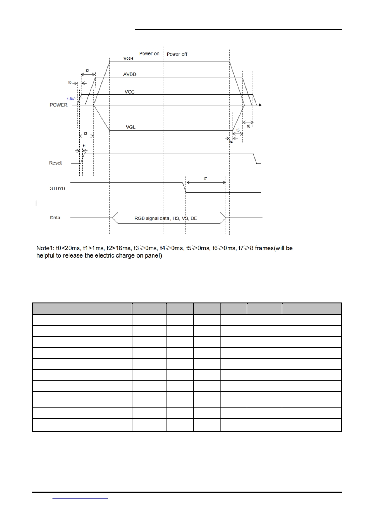
*1.Be sure to apply DVDD and VGL to the LCD first, and then apply VGH.
*2: DVDD setting should match the signals output voltage (refer to Note 3) of customer’s system board.
*3: DCLK,HS,VS,RESET,U/D, L/R,DE,R0~R7,G0~G7,B0~B7,MODE,DITHB.
6.2
Current Consumption
Items
Symbol
Min.
Typ.
Max.
Unit
Remark
I GH
0.05
0.2
1.0
mA
VGH = 15.0V
Current for Driver
I GL
0.2
0.5
1.0
mA
VGL = -10.0V
I DVDD
1
4.0
10
mA
DVDD=3.3V
I AVDD
5
20
30
mA
AVDD=10.4V
Document Name: LMT070DNCFWD-NNA-Manual-Rev0.1.DOC
Page: 5 of 15
TOPWAY
LCD Module User Manual
LMT070DNCFWD-NNA
6.3
LED Backlight Circuit Characteristics
Top=25¡æ
Items
Symbol
MIN.
TYP.
MAX.
Unit
Note
Forward Voltage
Vf BLA
9.0
9.6
10.5
V
If=100mA
Forward Current
If BLA
-
100.0
-
mA
Cautions:
Exceeding the recommended driving current could cause substantial damage to the backlight and shorten its lifetime.
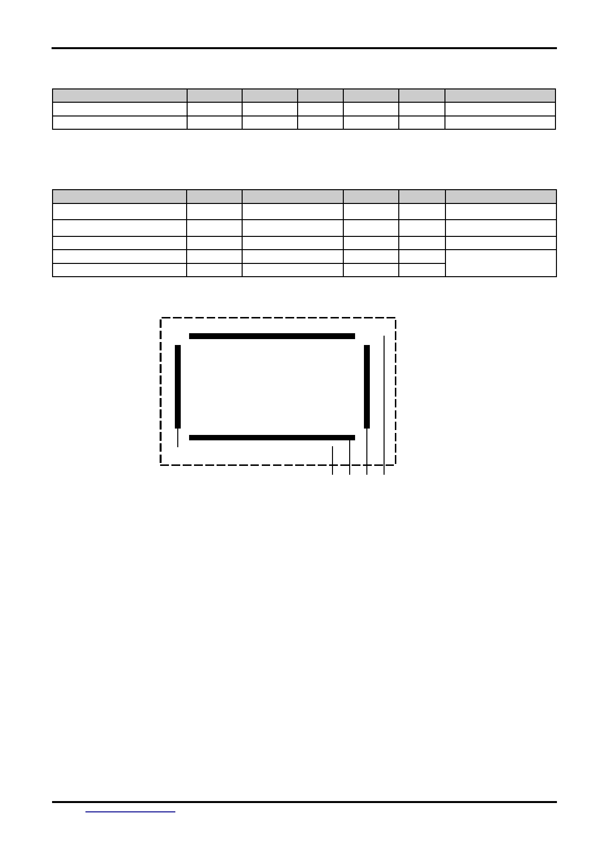
6.4
Touch Panel Characteristics
Items
MIN.
TYP.
MAX.
Unit
Note
Operating Voltage
-
5.0
-
V
-
Operating Force
100
-
160
g
-
Life Time
-
1,000,000
-
times
-
X Resistance
100
-
400
Ω
-
Y Resistance
450
-
950
Ω
Touch Panel Logic Details
YU
XL
XR
YD
Document Name: LMT070DNCFWD-NNA-Manual-Rev0.1.DOC
Page: 6 of 15
TOPWAY
LCD Module User Manual
LMT070DNCFWD-NNA
6.5
Power Sequence
7. AC Characteristics
7.1
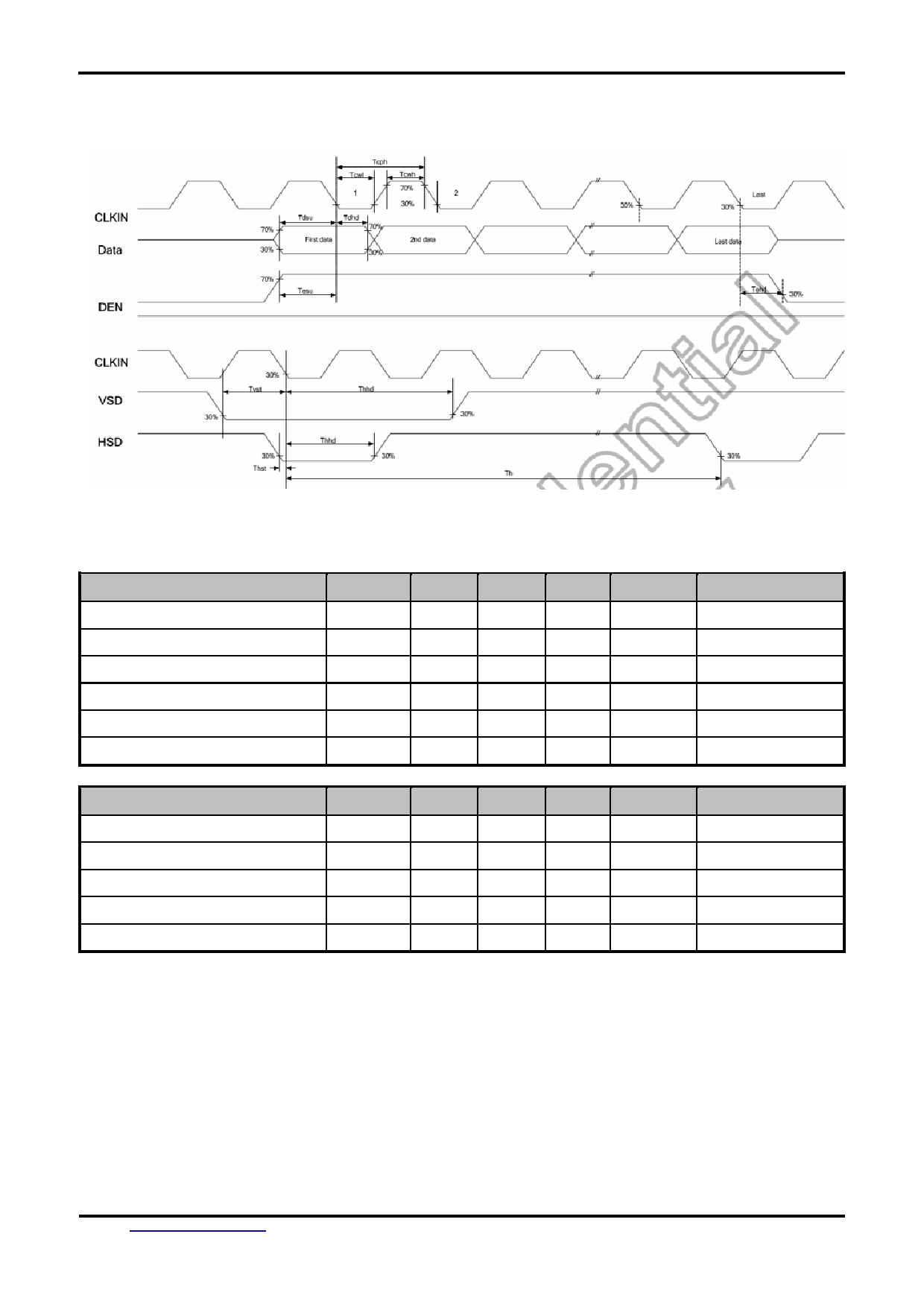
Timing Characteristics
Item
Symbol
MIN.
TYP.
MAX.
Unit
Remark
HS setup time
Thst
8
-
-
ns
HS hold time
Thhd
8
-
-
ns
VS setup time
Tvst
8
-
-
ns
VS hold time
Tvhd
8
-
-
ns
Data setup time
Tdsu
8
-
-
ns
Data hole time
Tdhd
8
-
-
ns
DE setup time
Tesu
8
-
-
ns
DV DD Power On Slew rate
TPOR
-
-
20
ms
From 0 to 90%
DV DD
DCLK cycle time
Tcph
20
-
-
ns
DCLK pulse duty
Tcwh
40
50
60
%
Note: For the details of the timing, please see the Driver IC data sheet.
Document Name: LMT070DNCFWD-NNA-Manual-Rev0.1.DOC
Page: 7 of 15
TOPWAY
LCD Module User Manual
LMT070DNCFWD-NNA
7.2
Input Clock and Data Timing Diagram
7.3
Timing
Item
Symbol
MIN.
TYP.
MAX.
Unit
Remark
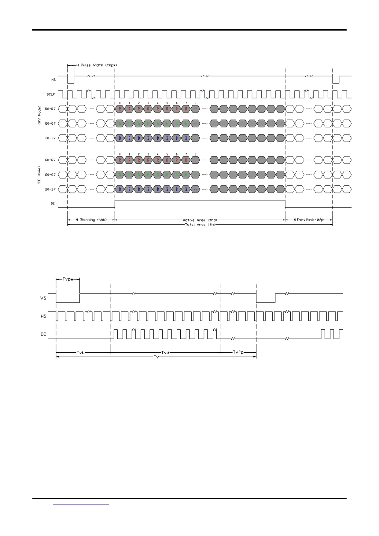
Horizontal Display Area
thd
-
800
-
DCLK
DCLK Frequency
fclk
28
33.3
40
MHz
One Horizontal Line
th
862
1056
1200
DCLK
HS pulse width
thpw
1
-
40
DCLK
HS Blanking
thb
46
46
46
DCLK
HS Front Porch
thfp
16
210
354
DCLK
Item
Symbol
MIN.
TYP.
MAX.
Unit
Remark
Vertical Display Area
tvd
-
480
-
TH
VS period time
tv
513
525
650
TH
VS pulse width
tvpw
1
-
20
TH
VS Blanking
tvb
23
23
23
TH
VS Front Porch
tvfp
7
22
147
TH
Document Name: LMT070DNCFWD-NNA-Manual-Rev0.1.DOC
Page: 8 of 15
TOPWAY
LCD Module User Manual
LMT070DNCFWD-NNA
7.4
Data Input Format
Figure 6-2-1 Horizontal input timing diagram.
Figure 6-2-2 Vertical input timing diagram.
Document Name: LMT070DNCFWD-NNA-Manual-Rev0.1.DOC
Page: 9 of 15
TOPWAY
LCD Module User Manual
LMT070DNCFWD-NNA
7.5
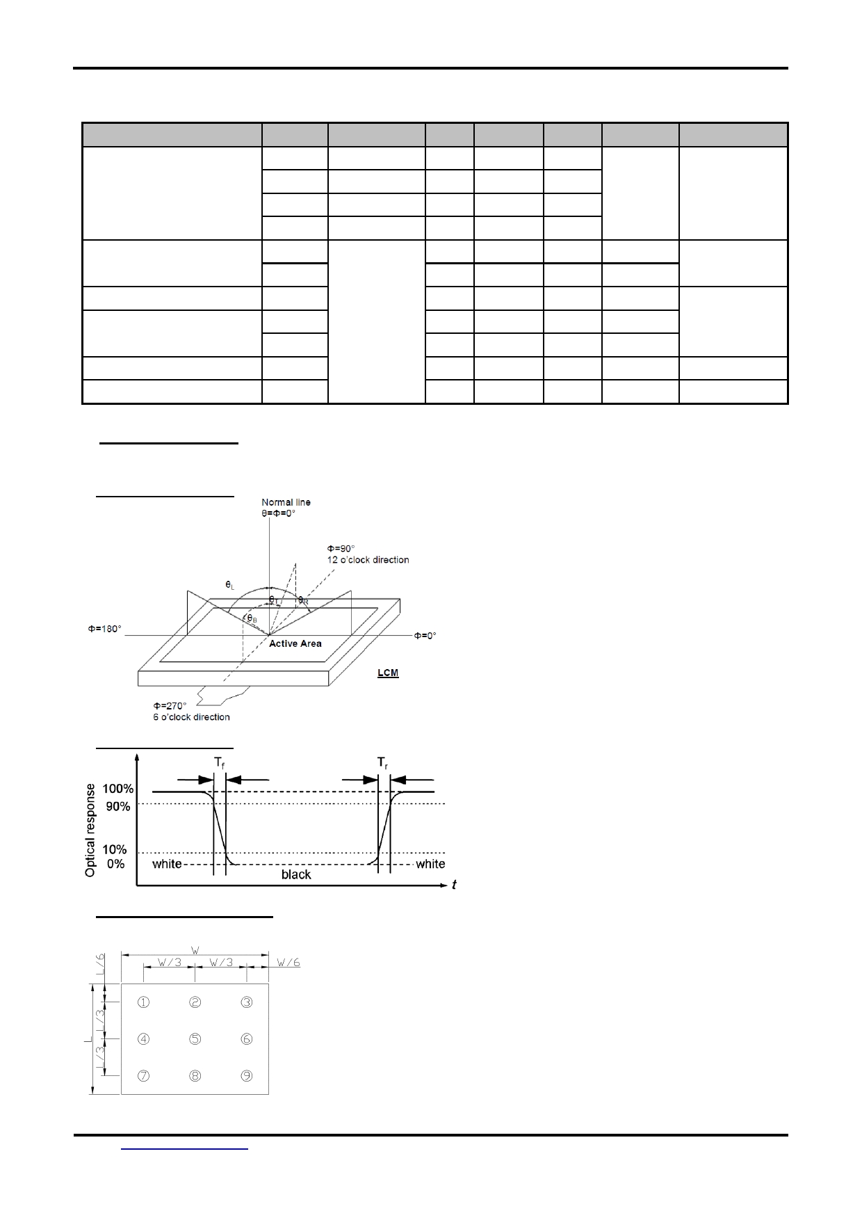
Optical Characteristics
Item
Symbol
Condition
MIN.
TYP.
MAX.
UNIT
Note.
θ L
9 o’clock
60
70
-
Viewing angle
θ R
3 o’clock
60
70
-
(CR¡Ý10)
degree
*2
θ T
12 o’clock
40
50
-
θ B
6 o’clock
60
70
-
T f
-
10
20
msec
Response Time
*3
T r
-
15
30
msec
Contrast ratio
CR
400
500
-
-
Normal
W X
0.26
0.31
0.26
-
*1
Color chromaticlty
θ =0 o
W Y
0.28
0.33
0.38
-
cd/m
2
Luminance
L
-
200
-
*4
Luminance uniformity
Y U
40
50
-
%
*4
Note:
*1. Definition of Contrast Ratio
The contrast ratio could be calculate by the following expression:
Contrast Ratio (CR) = Luminanc with all pixels white / Luminance with all pixels black
*2 Definition of Viewing Angle
*3 Definition of response time
*4 Definition of Luminance Uniformity
Luminance uniformity (Lu)=
Min. Luminance form pt1~pt9 / Max Luminance form Pt1~pt9
Document Name: LMT070DNCFWD-NNA-Manual-Rev0.1.DOC
Page: 10 of 15

TOPWAY
LCD Module User Manual
LMT070DNCFWD-NNA
8. LCD Module Design and
8. Òº¾§ÏÔʾģ¿éÉè¼ÆºÍʹÓÃÐëÖª
Handling Precautions
- Please ensure V0, VCOM is adjustable, to enable LCD module get
-
Çë×¢ÒâV0, VCOM µÄÉ趨, ÒÔÈ·±£Òº¾§ÏÔʾģ¿éÔÚ²»Í¬
the best contrast ratio under different temperatures, view angles
µÄʹÓÃζÈÏÂÒÔ¼°ÔÚ²»Í¬µÄÊӽǺÍλÖù۲ìÄ£¿éÏÔ
and positions.
ʾ£¬¾ùÄÜ´ïµ½×î¼Ñ¶Ô±È¶È£¬ÇëÎñ±Ø½«Ó¦Óõç·ÉÏÉèÖÃ
- Normally display quality should be judged under the best contrast
Ϊ¶Ô±È¶È¿Éµ÷¡£
ratio within viewable area. Unexpected display pattern may com out
-
Çë×¢ÒâÒº¾§ÏÔʾģ¿éµÄÏÔʾƷÖÊÅж¨ÊÇÖ¸ÔÚÕý³£¶Ô±È
under abnormal contrast ratio.
¶ÈÏÂÒÔ¼°ÊÓ´°(V.A)·¶Î§ÄÚ½øÐеģ¬·ÇÕý³£¶Ô±È¶ÈÏÂÒº
- Never operate the LCD module exceed the absolute maximum
¾§¿ÉÄÜ»á³öÏÖ·ÇÔ¤ÆÚµÄÏÔʾ²»Á¼£¬Ó¦×¢ÒâÇø·Ö¡£
ratings.
-
ÇëÎðÔÚ×î´ó¶î¶¨ÖµÒÔÍâʹÓÃÒº¾§ÏÔʾģ¿é¡£
- Never apply signal to the LCD module without power supply.
- Keep signal line as short as possible to reduce external noise
-
ÇëÎðÔÚûÓнÓͨµçÔ´µÄÌõ¼þÏ£¬¸øÒº¾§ÏÔʾģ¿éÊäËÍ
interference.
Ðźš£
- IC chip (e.g. TAB or COG) is sensitive to light. Strong light might
-
Ç뾡¿ÉÄÜËõ¶ÌÐźÅÏßµÄÁ¬½Ó£¬ÒÔ±ÜÃâ¶ÔÒº¾§ÏÔʾģ¿é
cause malfunction. Light sealing structure casing is recommended.
µÄÐźŸÉÈÅ¡£
-
¼¯³Éµç·ÒòIC о Ƭ( ÈçTAB»òCOG)¶Ô×ÏÍâÏß¼«ÎªÃô
- Make sure there is enough space (with cushion) between case and
¸Ð£¬Ç¿¹â»·¾³Ï¿ÉÄÜ»áÒýÆðÒº¾§ÏÔʾģ¿é¹¦ÄÜʧЧ£¬
LCD panel, to prevent external force passed on to the panel;
otherwise that may cause damage to the LCD and degrade its
¹ÊÓ¦²ÉÓò»Í¸¹âµÄÍâ¿Ç¡£
display result.
-
ÇëÔÚÒº¾§ÏÔʾģ¿éÓëÍâ¿ÇÖ®¼ä±£Áô×ã¹»µÄ¿Õ¼
- Avoid showing a display pattern on screen for a long time
³Äµæ)£¬ÒÔ»º³åÍâÁ¦¶ÔÒº¾§ÏÔʾģ¿éµÄË𻵻òÒòÊÜÁ¦²»
(continuous ON segment).
¾ù¶ø²úÉúµÄÏÔʾ²»ÔȵÈÒì³£ÏÖÏó¡£
- LCD module reliability may be reduced by temperature shock.
-
±ÜÃâÒº¾§ÏÔʾÆÁÔÚijһ»-Ãæϳ¤Ê±¼äµãÁÁ£¬·ñÔòÓгö
- When storing and operating LCD module, avoids exposure to direct
sunlight, high humidity, high or low temperature. They may damage
ÏÖ²ÐÓ°µÄ·çÏÕ£»Çëͨ¹ýÈí¼þÿ¸ôÒ»¶Îʱ¼ä¸Ä±äÒ»´Î»-
or degrade the LCD module.
Ãæ¡£
- Never leave LCD module in extreme condition (max./min
-
Òº¾§ÏÔʾģ¿éµÄ¿É¿¿ÐÔ¿ÉÄÜÒòζȳå»÷¶ø½µµÍ¡£
storage/operate temperature) for more than 48hr.
-
ÇëÎðÔÚÑô¹âÖ±Éä¡¢¸ßʪ¡¢¸ßλòµÍÎÂÏ´¢´æºÍʹÓÃÒº
- Recommend LCD module storage conditions is 0 C~40 C
¾§ÏÔʾģ¿é£¬Õ⽫Ôì³ÉÒº¾§ÏÔʾģ¿éµÄË𻵻òʧЧ¡£
<80%RH.
- LCD module should be stored in the room without acid, alkali and
harmful gas.
-
ÇëÎðÔÚ¼«ÏÞ»·¾³(×î´ó/ ×îС´æ´¢/ ¹¤×÷ζÈ)ÏÂʹÓûò
- Avoid dropping & violent shocking during transportation, and no
excessive pressure press, moisture and sunlight.
- Òº¾§ÏÔʾģ¿é½¨Òé´æ´¢Ìõ¼þΪ:0 C ~40 C <80%RH¡£
- LCD module can be easily damaged by static electricity. Please
-
ÇëÎðÈÃÒº¾§ÏÔʾģ¿é´æ´¢ÓÚ´øÓÐ
ËáÐÔ,¼îÐ Ô, Óк¦Æø
maintain an optimum anti-static working environment to protect the
Ìå»·¾³Ö®ÖС£
LCD module. (eg. ground the soldering irons properly)
-
ÔÚÔËÊä¹ý³ÌÖÐ,ÇëÎðÈÃÒº¾§ÏÔʾģ¿éµøÂäÓëÃÍÁÒÕð¶¯,
- Be sure to ground the body when handling LCD module.
- Only hold LCD module by its sides. Never hold LCD module by
ͬʱ±ÜÃâ Òì³£¼·Ñ¹, ¸ßʪ¶È, ÓëÑô¹âÕÕÉä.
applying force on the heat seal or TAB.
-
Òº¾§ÏÔʾģ¿é¼«Ò×Êܾ²µçË𻵣¬ÇëÎñ±Ø±£Ö¤Òº¾§ÏÔʾ
- When soldering, control the temperature and duration avoid
Ä£¿éÔÚ·À¾²µçµÄ¹¤×÷»·¾³ÖÐʹÓûò±£´æ ¡£(Èç: ÀÓÌúÕý
damaging the backlight guide or diffuser which might degrade the
È·½ÓµØ,µÈ)
display result such as uneven display.
-
ÄÃÈ¡Òº¾§ÏÔʾģ¿éʱÐè×¢Òâ²Ù×÷ÈËÔ±µÄ½ÓµØÇé¿ö¡£
- Never let LCD module contact with corrosive liquids, which might
-
ÇëÊÖ³ÖÒº¾§ÏÔʾģ¿éµÄ±ßÑØÈ¡·ÅÄ£¿é£¬·ÀÖ¹ÈÈѹֽ»ò
cause damage to the backlight guide or the electric circuit of LCD
module.
TAB²¿Î»ÊÜÁ¦¡£
- Only clean LCD with a soft dry cloth, Isopropyl Alcohol or Ethyl
-
º¸½ÓÒº¾§Ä£¿éʱ£¬Çë×¢Òâ¿ØÖÆÀÓÌúµÄζȡ¢º¸½Óʱ
Alcohol. Other solvents (e.g. water) may damage the LCD.
¼ä£¬ÒÔÃâÌÌ»µµ¼¹â°å»òÆ«¹âƬ£¬µ¼ÖÂÏÔʾ²»ÔȵȲ»Á¼
- Never add force to components of LCD module. It may cause
ÏÖÏó·¢Éú¡£
invisible damage or degrade the module's reliability.
-
ÇëÎðʹÓÃÏ´°åË®µÈ¸¯Ê´ÐÔÒºÌå½Ó´¥Òº¾§Ä£¿é£¬ÒÔÃⸯ
- When mounting LCD module, please make sure it is free from
Ê´µ¼¹â°å»òÄ£¿éµç·¡£
twisting, warping and bending.
- Do not add excessive force on surface of LCD, which may cause
the display color change abnormally.
-
½ö¿ÉʹÓÃÈáÈíµÄ¸É²¼,Òì±û´¼»òÒÒ´¼Çå½àÒº¾§ÆÁ±í
- LCD panel is made with glass. Any mechanical shock (e.g.
Ã棬ÆäËûÈκÎÈܼÁ(Èç:Ë®)¶¼ÓпÉÄÜËð»µÒº¾§Ä£¿é¡£
Document Name: LMT070DNCFWD-NNA-Manual-Rev0.1.DOC
Page: 11 of 15
TOPWAY
LCD Module User Manual
LMT070DNCFWD-NNA
dropping from high place) will damage the LCD module.
-
ÇëÎð¼·Ñ¹Òº¾§ÏÔʾģ¿éÉϵÄÔªÆ÷¼þ£¬ÒÔ±ÜÃâ²úÉúDZÔÚ
µÄË𻵻òʧЧ¶øÓ°Ïì²úÆ·¿É¿¿ÐÔ¡£
-
×°ÅäÒº¾§ÏÔʾģ¿éʱ£¬ÇëÎñ±Ø×¢Òâ±ÜÃâÒº¾§ÏÔʾģ¿é
µÄŤÇú»ò±äÐΡ£
-
ÇëÎð¼·Ñ¹Òº¾§ÏÔʾÆÁ±íÃ棬Õ⽫µ¼ÖÂÏÔʾÑÕÉ«µÄÒì
³£¡£
-
Òº¾§ÆÁÓɲ£Á§ÖÆ×÷¶ø³É£¬ÈκλúеÅöײ(Èç´Ó¸ß´¦µø
Âä)¾ùÓпÉÄÜËð»µÒº¾§ÏÔʾģ¿é¡£
- Protective film is attached on LCD screen. Be careful when peeling
-
Òº¾§ÆÁ±íÃæ´øÓб£»¤Ä¤, ½Ò³ý±£»¤Ä¤Ê±ÐèҪעÒâ¿ÉÄÜ
off this protective film, since static electricity may be generated.
²úÉúµÄ¾²µç¡£
- Polarizer on LCD gets scratched easily. If possible, do not remove
-
ÒòÒº¾§ÏÔʾÆÁ±íÃæµÄÆ«¹âƬ¼«Ò×»®ÉË£¬°²×°Íê³É֮ǰ
LCD protective film until the last step of installation.
Ç뾡Á¿²»Òª½Òϱ£»¤Ä¤¡£
- When peeling off protective film from LCD, static charge may cause
-
Ç뻺Âý½Ò³ý±£»¤Ä¤£¬Ôڴ˹ý³ÌÖÐÒº¾§ÏÔʾÆÁÉÏ¿ÉÄÜ»á
abnormal display pattern. The symptom is normal, and it will turn
²úÉú¾²µçÏߣ¬´ËΪÕý³£Çé¿ö£¬¿ÉÔÚ¶Ìʱ¼äÄÚÏûʧ¡£
back to normal in a short while.
- LCD panel has sharp edges, please handle with care.
-
Çë×¢Òâ±ÜÃâ±»Òº¾§ÏÔʾÆÁµÄ±ßÔµ¸îÉË¡£
- Never attempt to disassemble or rework LCD module.
-
Çë²»ÒªÊÔͼ²ðж»ò¸ÄÔìÒº¾§ÏÔʾģ¿é¡£
- If display panel is damaged and liquid crystal substance leaks out,
-
µ±Òº¾§ÏÔʾÆÁ³öÏÖÆÆÁÑ,ÄÚ²¿Òº¾§ÒºÌå¿ÉÄÜÁ÷³ö;
be sure not to get any in your mouth, if the substance comes into
¹ØÒºÌå²»¿ÉÍ̳Ô, ¾ø¶Ô²»¿É½Ó´¥×ì°Í, Èç½Ó´¥µ½Æ¤·ô
contact with your skin or clothes promptly wash it off using soap
»òÒ·þ, ÇëʹÓ÷ÊÔíÓëÇåË®³¹µ×ÇåÏ´.
and water.
9. CTP Mounting Instructions
9. µçÈÝ´¥ÃþÆÁ°²×° Ö¸µ¼
9.1 Ãæ¿ò°²×°£¨¸½Í¼
1£©
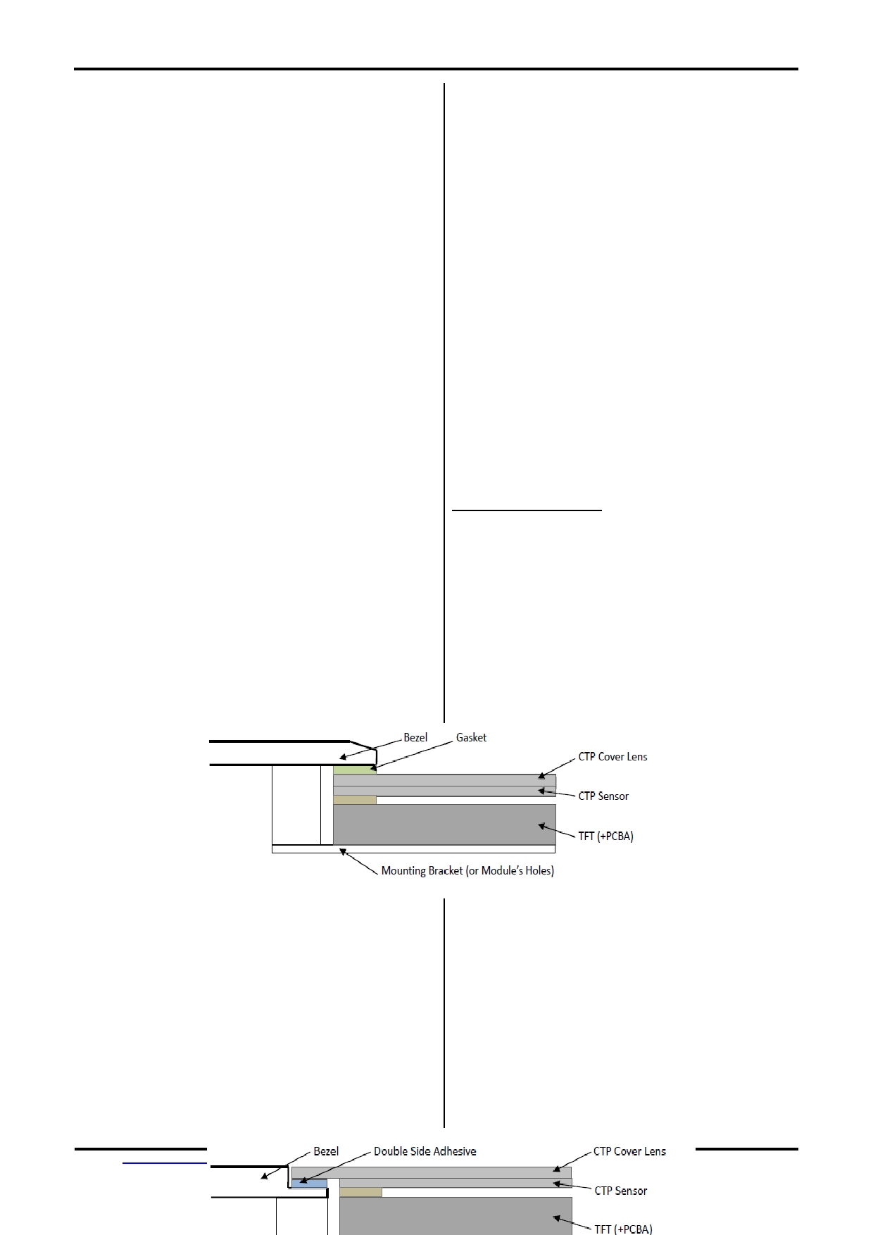
9.1 Bezel Mounting (Figure 1)
-
¿Í»§Ãæ¿ò´°¿ÚÓ¦´óÓÚCTP¶¯×÷ÇøÓò£¬¸÷±ßÀ붯×÷ÇøÓ¦
- The bezel window should be bigger than the CTP active area. It
¡Ý0.5mm.
should be¡Ý0.5mm each side.
-
Ãæ¿òÓëCTPÃæ°å¼äÓ¦µæÓнºµæ£¬Æä×îÖÕ¼ä϶ԼΪ0.5¡«
- Gasket should be installed between the bezel and the CTP surface.
1.0mm.
The final gap should be about 0.5~1.0mm.
-
½¨Òé±ØҪʱÔÚ±³ÃæÌṩ¸½¼ÓÖ§¼Ü(ÀýÈçÎÞ°²×°½á¹¹µÄ±¡
- It is recommended to provide an additional support bracket for
ÐÍ TFTÄ£¿é)£¬Ó¦½öÀûÓÃÊʵ±Ö§³ÅÒÔ±£³ÖÄ£¿éλÖÃ.
backside support when necessary (e.g. slim type TFT module
without mounding structure). They should only provide appropriate
support and keep the module in place.
-
°²×°½á¹¹Ó¦¾ßÓÐ×ã¹»µÄÇ¿¶È£¬ÒÔ·ÀÖ¹Íⲿ²»¾ùÔÈÁ¦»ò
- The mounting structure should be strong enough to prevent
ŤÇúÁ¦×÷Óõ½Ä£¿éÉÏ.
external uneven force or twist act onto the module.
Figure 1
9.2 Surface Mounting (Figure 2)
9.2 ǶÈë°²×°£¨¸½Í¼
2£©
- As the CTP assembling on the countersink area with double side
-
¿Í»§Ãæ¿òÓ¦¾ßÓÐʹÓÃË«Ã潺ճÌùCTPµÄ½á¹¹³Ą́Ã棬
adhesive.
ÆäÕ³ÌùÃæÒªÇóƽÕûÇҽྻÎÞÎÛÒÔ±£Ö¤Õ³ÌùÀο¿.
The countersink area should be flat and clean to ensure the double
side adhesive installation result.
- The Bezel is recommend to keep a gap (¡Ý 0.3mm each side)
-
¿¼Âǵ½ÖÆ×÷Îó²î£¬½¨ÒéÃæ¿òÓëCTP¸Ç°åÖ®¼äËÄÖÜÁôÓÐ
around the cover lens for tolerance.
¡Ý0.3mm¼ä϶.
- It is recommended to provide an additional support bracket with
-
½¨Òé±ØҪʱÔÚ±³ÃæÌṩµæÓнºµæ¸½¼ÓÖ§¼Ü(
gasket for backside support when necessary (e.g. TFT module
½á¹¹µÄTFTÄ£¿é)£¬Ó¦½öÀûÓÃÊʵ±Ö§³ÅÒÔ±£³ÖÄ£¿éλ
without mounding structure). They should only provide appropriate
ÖÃ.
support and keep the module in place.
- The mounting structure should be strong enough to prevent
-
°²×°½á¹¹Ó¦¾ßÓÐ×ã¹»µÄÇ¿¶È£¬ÒÔ·ÀÖ¹Íⲿ²»¾ùÔÈÁ¦»ò
external uneven force or twist act onto the module
ŤÇúÁ¦×÷Óõ½Ä£¿éÉÏ¡£
Document Name: LMT070DNCFWD-NNA-Manual-Rev0.1.DOC
Page: 12 of 15
TOPWAY
LCD Module User Manual
LMT070DNCFWD-NNA
Figure 2
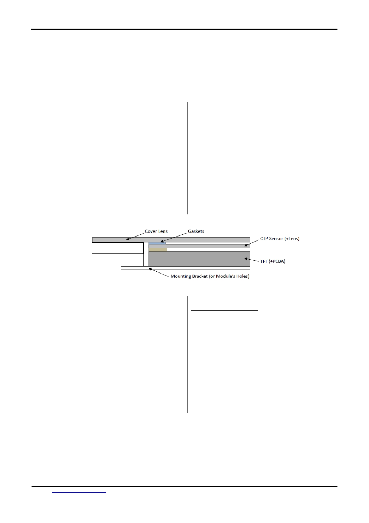
9.3 Additional Cover Lens Mounting (Figure 3)
9.3 ¸²¼Ó¸Ç°å£¨¸½Í¼
3£©
- For the case of additional cover Lens mounting, it is necessary to
-
ÐèÒª¸²¼Ó²£Á§¸Ç°åµÄ°²×°£¬ÎªÈ·±£Æ书ÄÜ£¬ÓбØÒª²é
recheck with the CTP specification about the material and thickness
¿´²úÆ·¹æ¸ñÊéÖÐÓйظǰå²ÄÁϺͺñ¶ÈµÄ˵Ã÷.
to ensure the functionality.
- It should keep a 0.2~0.3mm gap between the cover lens and the
-
²£Á§¸Ç°åÓëCTP±íÃæÖ®¼äÓ¦ÁôÓÐ0.2¡«0. 3mm¼ä϶.
CTP surface..
- The cover lens window should be bigger than the active area of the
-
²£Á§¸Ç°åÊÓ´°Ó¦´óÓÚCTP¶¯×÷ÇøÓò£¬¸÷±ßÀ붯×÷ÇøÓ¦
CTP.It should be¡Ý0.5mm each side.
¡Ý0.5mm¡£
- It is recommended to provide an additional support bracket for
-
½¨Òé±ØҪʱÔÚ±³ÃæÌṩ¸½¼ÓÖ§¼Ü(ÀýÈçÎÞ°²×°½á¹¹µÄ±¡
backside support when necessary (e.g. slim type TFT module
ÐÍ TFTÄ£¿é)£¬Ó¦½öÀûÓÃÊʵ±Ö§³ÅÒÔ±£³ÖÄ£¿éλÖÃ.
without mounding structure). They should only provide appropriate
support and keep the module in place.
- The mounting structure should be strong enough to prevent
-
°²×°½á¹¹Ó¦¾ßÓÐ×ã¹»µÄÇ¿¶È£¬ÒÔ·ÀÖ¹Íⲿ²»¾ùÔÈÁ¦»ò
external uneven force or twist act onto the module.
ŤÇúÁ¦×÷Óõ½Ä£¿éÉÏ.
Figure 3
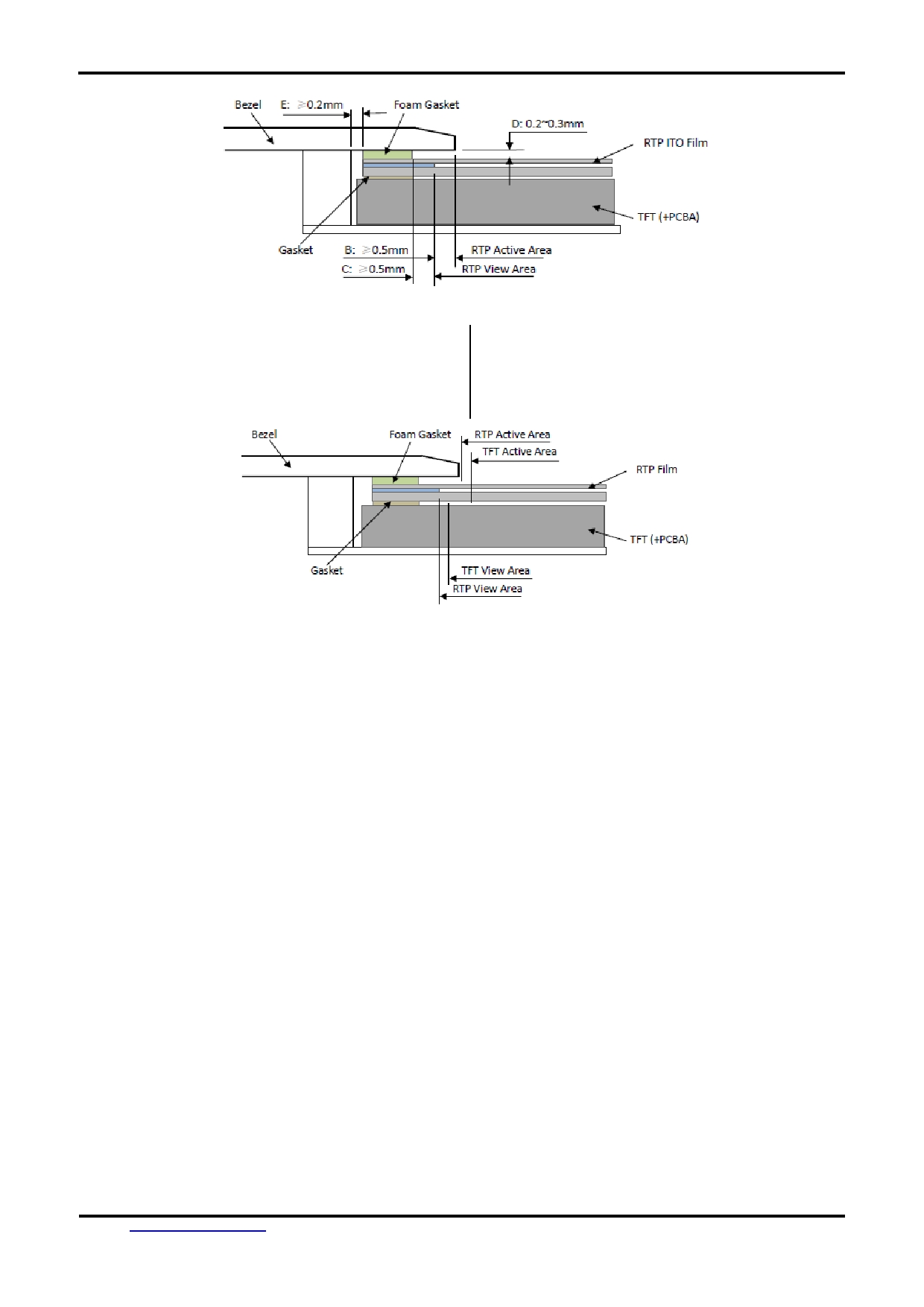
10. RTP Mounting Instructions
10. µç×è´¥ÃþÆÁ°²×°Ö¸µ¼
- Ϊ±ÜÃâÃæ¿òÖ±½ÓѹÔÚ¶¯×÷Çø(A.A.)ÉÏÔì³ÉÎó¶¯×÷£¬Ãæ¿ò
- It should bezel touching the RTP Active Area (A.A.) to prevent
Óëµç×è´¥ÃþÆÁ(RTP)Ö®¼äÓ¦ÁôÓÐÒ»¶¨µÄ¿Õ϶
abnormal touch.It should left gab D=0.2~0.3mm in between.
D=0.2~0.3mmÖ®¼ ä.( ¸½Í¼4)
(Figure 4)
- Outer bezel design should take care about the area outside the
- Éè¼ÆÃæ¿òʱ£¬Òª×¢ÒâÓÃÃæ¿ò±£»¤´¥ÃþÆÁËÄÖܵķDZ£Ö¤²Ù
A.A. Those areas contain circuit wires which is having different
×÷ÇøÓò£¬ÒòΪ²¼ÏßÇøÓòÔÚ´Ë´¦ÐγÉһ̨½×£¬ÔÚ´ËÇøÓò
thickness. Touching those areas could de-form the ITO film. As a
¸½½ü²Ù×÷ʱ ITO Film
±äÐνϴó£¬ÈÝÒ×µ¼Ö ITO Ë𻵶ø
result bezel the ITO film be damaged and shorten its lifetime.
½µµÍÊÙÃü¡£Îª±£»¤
RTPºÍ±ÜÃâÎó²Ù×÷£¬ÔÚ
RTP ÓëÃæ¿ò
It is suggested to protect those areas with gasket (between the
Ö®¼äµæ»º³åÎG asket £©£¬ÎÒÃǽ¨ÒéÉè¼ÆÃæ¿òÓ¦¸²¸Ç
bezel and RTP).The suggested figures are B ≥0.50mm; C≥0.50mm .
¶¯×÷ÇøµÄ±ßÔµ£¬Ãæ¿ò±ßÔµµ½V.A.ÇøµÄ¾àÀë B¡Ý0.50mm;
(Figure 4)
µæȦÄÚ±ßÔµµ½V.A.ÇøµÄ¾àÀë C¡Ý0.50mm . ( ¸½Í¼ 4)
- The bezel side wall should keep space E= 0.2 ~ 0.3mm from the
- ÔÚÉè¼ÆÃæ¿òÓëRTP ×éװʱ£¬Ó¦¿¼Âǵ½Ãæ¿òÄÚ²àÓëRTP Íâ
RTP. (Figure 4)
²àµÄ¼ä¾àE¡Ý0.2mm.
( ¸½Í¼ 4)
Document Name: LMT070DNCFWD-NNA-Manual-Rev0.1.DOC
Page: 13 of 15
TOPWAY
LCD Module User Manual
LMT070DNCFWD-NNA
Figure 4
- In general design,
- ͨ³£Éè¼Æʱ£º
RTP V.A. should be bigger than the TFT V.A.
RTPµÄ¿ÉÊÓÇø V.A.
Ó¦²»Ð¡ÓÚ TFT µÄ¿ÉÊÓÇø V.A.
and RTP A.A. should be bigger than the TFT A.A.
¼° RTP µÄ¶¯×÷Çø A.A.
Ó¦²»Ð¡ÓÚ TFT µÄ¶¯×÷Çø A.A.
(Figure 5)
( ¸½Í¼ 5)
Figure 5
Document Name: LMT070DNCFWD-NNA-Manual-Rev0.1.DOC
Page: 14 of 15

TOPWAY
LCD Module User Manual
LMT070DNCFWD-NNA
Warranty
This product has been manufactured to our company’s specifications as a part for use in your company’s general
electronic products. It is guaranteed to perform according to delivery specifications. For any other use apart from general
electronic equipment, we cannot take responsibility if the product is used in medical devices, nuclear power control
equipment, aerospace equipment, fire and security systems, or any other applications in which there is a direct risk to
human life and where extremely high levels of reliability are required. If the product is to be used in any of the above
applications, we will need to enter into a separate product liability agreement.
-
We cannot accept responsibility for any defect, which may arise form additional manufacturing of the product
(including disassembly and reassembly), after product delivery.
-
We cannot accept responsibility for any defect, which may arise after the application of strong external force to the
product.
-
We cannot accept responsibility for any defect, which may arise due to the application of static electricity after the
product has passed our company’s acceptance inspection procedures.
-
When the product is in CCFL models, CCFL service life and brightness will vary according to the performance of the
inverter used, leaks, etc. We cannot accept responsibility for product performance, reliability, or defect, which may
arise.
-
We cannot accept responsibility for intellectual property of a third part, which may arise through the application of our
product to our assembly with exception to those issues relating directly to the structure or method of manufacturing of
our product.
Document Name: LMT070DNCFWD-NNA-Manual-Rev0.1.DOC
Page: 15 of 15