TOPWAY
LCD Module User Manual
LMT070FNMFWA-NND-1
LMT070FNMFWA-NND-1
LCD Module User Manual
Prepared by:
Checked by:
Approved by:
Yurj
Date: 2019-10-10
Date:
Date:
Rev. Descriptions
Release Date
0.1
Preliminary release
2019-09-30
0.2
Update section 5.2
2019-10-10
URL: www.topwaydisplay.com
Document Name: LMT070FNMFWA-NND-1-Manual-Rev0.2
Page: 1 of 12

TOPWAY
LCD Module User Manual
LMT070FNMFWA-NND-1
Table of Content
1. General Specification ............................................................................................................ 3
2. Block Diagram ....................................................................................................................... 3
3. Terminal Function ................................................................................................................. 4
3.1
K1 LVDS Terminal ................................................................................................................................................ 4
4. Absolute Maximum Ratings .................................................................................................. 5
5. Electrical Characteristics ...................................................................................................... 5
5.1
DC Characteristics ................................................................................................................................................. 5
5.2
LED Backlight Circuit Characteristics ..................................................................................................................... 5
6. AC Characteristics ................................................................................................................ 6
6.1
AC Electrical Characteristics .................................................................................................................................. 6
6.2
DC Electrical Characteristics.................................................................................................................................. 7
6.3
Timing .................................................................................................................................................................... 8
6.4
Data Input Format .................................................................................................................................................. 8
6.5
Input Clock and Data Timing Diagram ................................................................................................................... 8
7. Optical Characteristics .......................................................................................................... 9
7.1
TFT Optical Characteristics ................................................................................................................................... 9
8. Touch panel Design Precautions ....................................................................................... 12
8.1
Mounting Precaution ............................................................................................................................................ 12
9. Precautions of using LCD Modules .................................................................................... 12
URL: www.topwaydisplay.com
Document Name: LMT070FNMFWA-NND-1-Manual-Rev0.2
Page: 2 of 12
TOPWAY
LCD Module User Manual
LMT070FNMFWA-NND-1
1. General Specification
Signal Interface :
LVDS ( VESA 24 bit )
Display Mode :
SFT Transmissive / Normally Black
Screen Size(Diagonal) :
7.0”
Outline Dimension :
195.8 x 116.0x 9.7(mm)
(see attached drawing for details)
Active Area :
154.21 x 85.92 (mm)
Number of dots :
1024 x 3 (RGB) x 600
Pixel Pitch :
0.1506 x 0.1432 (mm)
Pixel Configuration :
RGB Stripe
Backlight :
LED
Viewing Direction :
All
Touch Panel:
Capacitive Touch Panel
Touch Driver IC:
ILI2118A
Operating Temperature :
-20 ~ +70°C
Storage Temperature :
-30 ~ +80°C
Surface Treatment :
AF
2. Block Diagram
CTP_SCL, CTP_SDA,
CTP_INT, CTP_RESET
Capacitive Touch Panel
LED_ADODE
Backlight
LED_CATHODE
1024 x 600
Source Driver
RXIN0+, RXIN0-, RXIN1+, RXIN1-
RXIN2+, RXIN2-, RXIN3+, RXIN3-
RXCLKIN-, RXCLKIN+
LVDS interface
Power Circuit
VDD, GND, VGL, VGH, AVDD
URL: www.topwaydisplay.com
Document Name: LMT070FNMFWA-NND-1-Manual-Rev0.2
Page: 3 of 12

TOPWAY
LCD Module User Manual
LMT070FNMFWA-NND-1
3. Terminal Function
3.1 K1 LVDS Terminal
Pin No.
Pin Name
I/O
Descriptions
1
NC
---
No connection
2
VDD
P
Power Voltage for LCD digital circuit(3.3V)
3
RESET
I
Global reset pin, low active
4
VGH
P
Gate ON Voltage
5
VGL
P
Gate OFF Voltage
6
AVDD
P
Power for Analog Circuit
7
GND
P
Ground
8
RXIN0-
I
- LVDS differential data input
9
RXIN0+
I
+LVDS differential data input
10
GND
P
Ground
11
RXIN1-
I
-LVDS differential data input
12
RXIN1+
I
+LVDS differential data input
13
GND
P
Ground
14
RXIN2-
I
-LVDS differential data input
15
RXIN2+
I
+LVDS differential data input
16
GND
P
Ground
17
RXCLKIN-
I
-LVDS differential clock input
18
RXCLKIN+
I
+LVDS differential clock input
19
GND
P
Ground
20
RXIN3-
I
-LVDS differential data input
21
RXIN3+
I
+LVDS differential data input
22
GND
P
Ground
23
VDD
P
Power Voltage for CTP digital circuit(3.3V)
24
GND
P
Ground
25
NC
---
No connection
26
NC
---
No connection
27
CTP_SCL
I
I2C clock input
28
CTP_SDA
I/O
I2C data input and output
29
CTP_INT
O
Interrupt signal from the TP IC
30
CTP_RESET
I
Reset pin for CTP, low active
31
LED_A
P
LED Anode
32
LED_A
P
LED Anode
33
GND
P
Ground
34
LED_K
P
LED Cathode
35
LED_K
P
LED Cathode
36
LED_K
P
LED Cathode
37
LED_K
P
LED Cathode
38
LED_K
P
LED Cathode
39
LED_K
P
LED Cathode
40
GND
P
Ground
Note 1: I/O definition.
I---Input pin, O---Output pin, P--- Power/Ground, N--- No Connection
URL: www.topwaydisplay.com
Document Name: LMT070FNMFWA-NND-1-Manual-Rev0.2
Page: 4 of 12
TOPWAY
LCD Module User Manual
LMT070FNMFWA-NND-1
4. Absolute Maximum Ratings
Items
Symbol
Min.
Max.
Unit
Condition
Power voltage
V DD
-0.3
3.6
V
Operating Temperature
T OP
-20
70
C
No Condensation
Storage Temperature
T ST
-30
80
C
No Condensation
Note:
*1. This rating applies to all parts of the module. And should not be exceeded.
*2. The operating temperature only guarantees operation of the circuit. The contrast, response speed,
and the other specification related to electro-optical display quality is determined at the room temperature, T OP =25 ℃
*3. Ambient temperature when the backlight is lit (reference value)
*4. Any Stresses exceeding the Absolute Maximum Ratings may cause substantial damage to the device. Functional operation of this device at
other conditions beyond those listed in the specification is not implied and prolonged exposure to extreme conditions may affect device
reliability.
5. Electrical Characteristics
5.1 DC Characteristics
Items
Symbol
Min.
Typ.
Max.
Unit
Remark
VDD
3.0
3.3
3.6
V
Power voltage
AVDD
10.2
10.4
10.6
V
VGH
14.5
15.0
15.5
V
VGL
-10.5.
-10.0
-9.5
V
Input logic high voltage
VIH
2.3
-
3.3
V
Input logic low voltage
VIL
0
-
0.5
V
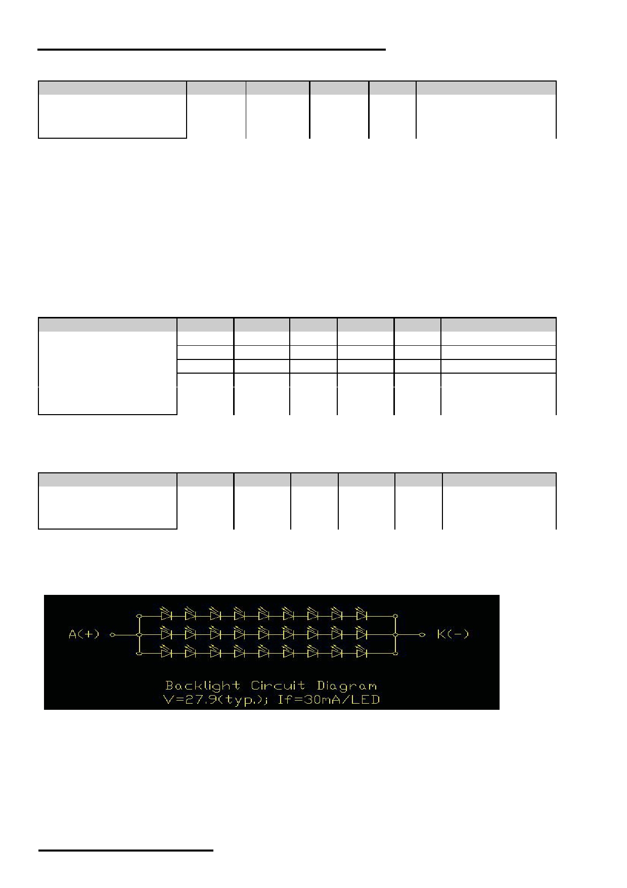
5.2 LED Backlight Circuit Characteristics
Top=25 ℃
Items
Symbol
MIN.
TYP.
MAX.
Unit
Note
Forward Voltage
Vf BLA
27
27.9
28.8
V
If=90mA
Forward Current
If BLA
-
90
-
mA
Operating Life Time
-
30000
-
Hrs
Cautions:
Exceeding the recommended driving current could cause substantial damage to the backlight and shorten its lifetime.
I F is defined for one channel LED. Optical performance should be evaluated at Ta=25 only If LED is driven by high current, high
ambient temperature & humidity condition. The life time of LED will be reduced. Operating life means brightness goes down to
50% initial brightness. Typical operating life time is estimated data.
URL: www.topwaydisplay.com
Document Name: LMT070FNMFWA-NND-1-Manual-Rev0.2
Page: 5 of 12

TOPWAY
LCD Module User Manual
LMT070FNMFWA-NND-1
6. AC Characteristics
6.1 AC Electrical Characteristics
Parameter
Symbol
Min
Typ
Max
Unit
Conditions
Clock Frequency
RxFCLK
20
-
71
MHz
Input data skew margin
TRSKM
-
500
ps
Clock high time
TLVCH
4/(7* R xFCLK )
ns
Clock low time
TLVCL
3/(7* R xFCLK )
ns
PLL wake-up time
TenPLL
150
us
URL: www.topwaydisplay.com
Document Name: LMT070FNMFWA-NND-1-Manual-Rev0.2
Page: 6 of 12
TOPWAY
LCD Module User Manual
LMT070FNMFWA-NND-1
6.2 DC Electrical Characteristics
VDD=3.3V, AVDD=9.6V, AGND=GND=0V, Ta=25
Parameter
Symbol
Min
Typ
Max
Unit
Remark
Differential input
high Threshold
RXVTH
–
–
+0.2
V
voltage
Differential input
Low Threshold
RXVTL
-0.2
–
–
V
voltage
Input voltage range
RXVIN
0
–
VDD-1.2
V
Differential input
common
RXVCM |V ID |/2
–
VDD-1.2+
V
Mode voltage
|V ID |/2
Differential input
voltage
|V ID |
0.2
v
0.6
V
Differential input
leakage Current
RVXliz
-10
v
+10
uA
LVDS Digital
Operating Current
Iddlvds
–
15
30
mA Fclk=65MHz,VDD=3.3V
LVDS Digital
Clock & all functions are
Stand-by Current
Istlvds
–
10
50
uA
stopped
URL: www.topwaydisplay.com
Document Name: LMT070FNMFWA-NND-1-Manual-Rev0.2
Page: 7 of 12
TOPWAY
LCD Module User Manual
LMT070FNMFWA-NND-1
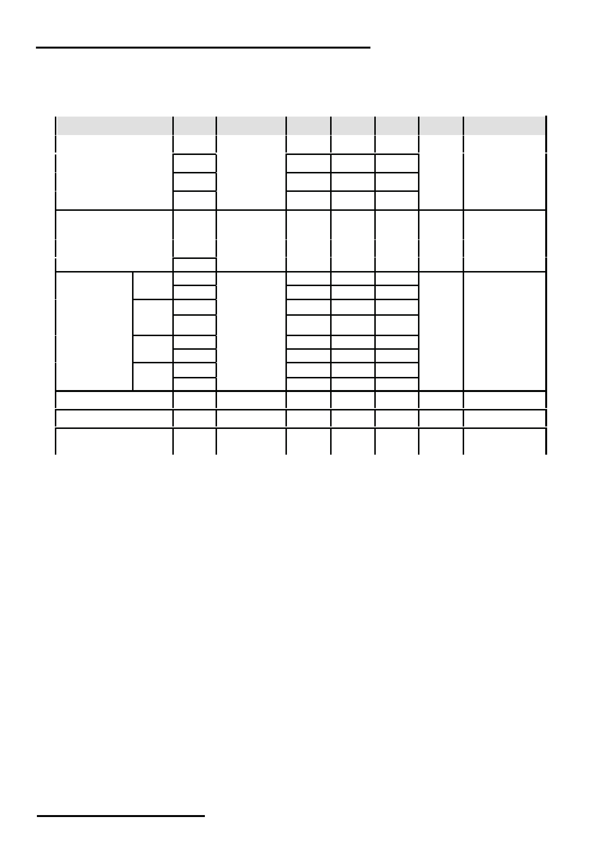
6.3 Timing
Parameter
Symbol
Min
Typ
Max
Unit
Remark
Clock
Frame
frequency
fclk
44.9
51.2
63
MHz
rate=60Hz
Horizontal
display area
thd
1024
DCLK
HS period
time
th
1200
1344
1400
DCLK
HS Blanking
thbp+thfp
176
320
376
DCLK
Vertical
display area
tvd
600
H
VS period
time
tv
616
760
816
H
VS Blanking
tvbp+tvfp
16
160
216
H
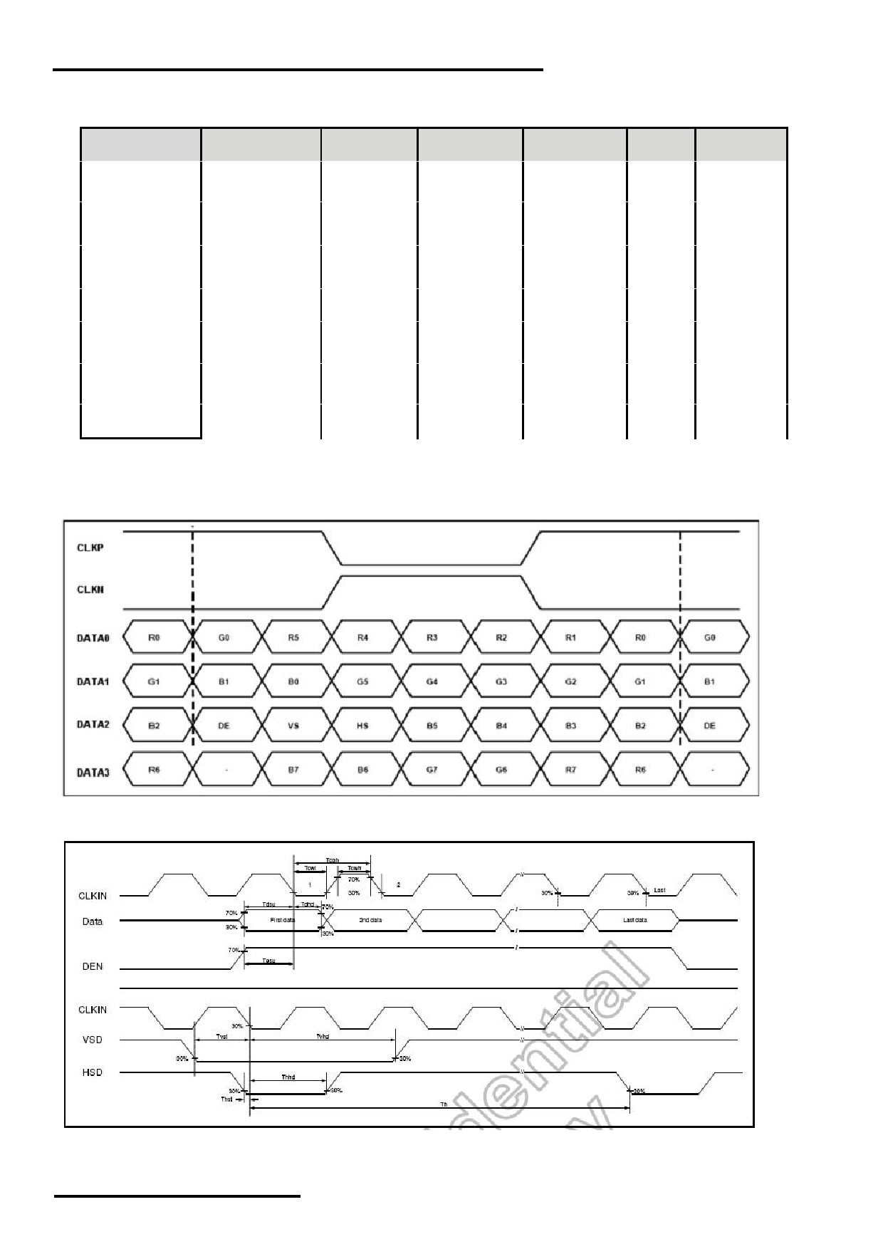
6.4 Data Input Format
6.5 Input Clock and Data Timing Diagram
URL: www.topwaydisplay.com
Document Name: LMT070FNMFWA-NND-1-Manual-Rev0.2
Page: 8 of 12
TOPWAY
LCD Module User Manual
LMT070FNMFWA-NND-1
7. Optical Characteristics
7.1 TFT Optical Characteristics
Item
Symbol Condition
Min
Typ
Max
Unit
Remark
θT
70
85
-
θB
70
85
-
View Angles
CR 10
Degree Note 2
θL
70
85
-
θR
70
85
-
Left/right 0
Contrast Ratio
CR
θ=0°
600
800
-
Top/bottom 5
Response Time
T ON
25
-
25
35
ms
Note1
T OFF
Note4
x
0.300 0.305 0.310
White
y
0.3058 0.3108 0.3158
x
0.553
0.603 0.653
Red
Chromaticity
y
0.310
0.360 0.410
Note5
x
0.300
0.350 0.400
Note1
Green
y
0.523
0.573 0.623
x
0.100
0.150 0.200
Blue
Backlight is
y
on
0.060
0.110 0.160
Uniformity
U
70
75
-
%
Note1 Note6
NTSC
45
50
-
%
Luminance
L
800
-
-
cd/m 2
Note7
Test Conditions:
1. I F = 90 mA, and the ambient temperature is 25 .
2. The test systems refer to Note 1 and Note 2.
URL: www.topwaydisplay.com
Document Name: LMT070FNMFWA-NND-1-Manual-Rev0.2
Page: 9 of 12
TOPWAY
LCD Module User Manual
LMT070FNMFWA_NNA
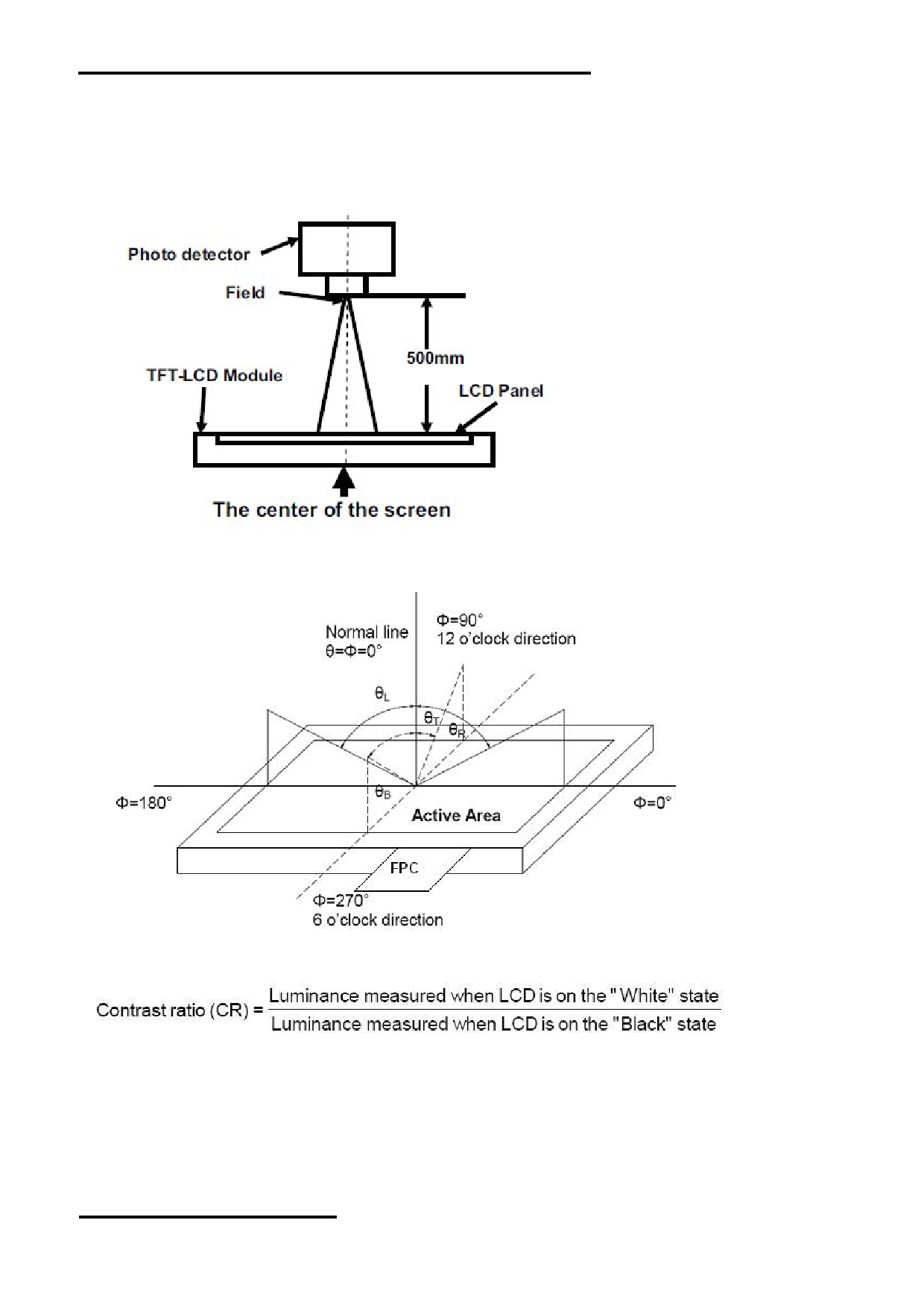
Note 1: Definition of optical measurement system.
The optical characteristics should be measured in dark room. After 5 Minutes operation, the optical
properties are measured at the center point of the LCD screen. All input terminals LCD panel must
be ground when measuring the center area of the panel.
Note 2: Definition of viewing angle range and measurement system.
viewing angle is measured at the center point of the LCD by CONOSCOPE(ergo-80)
Note 3: Definition of contrast ratio
“White state “: The state is that the LCD should drive by Vwhite.
“Black state”: The state is that the LCD should drive by Vblack.
Vwhite: To be determined
Vblack: To be determined.
URL: www.topwaydisplay.com
Document Name: LMT070FNMFWA-NND-1-Manual-Rev0.2
Page: 10 of 12
TOPWAY
LCD Module User Manual
LMT070FNMFWA_NNA
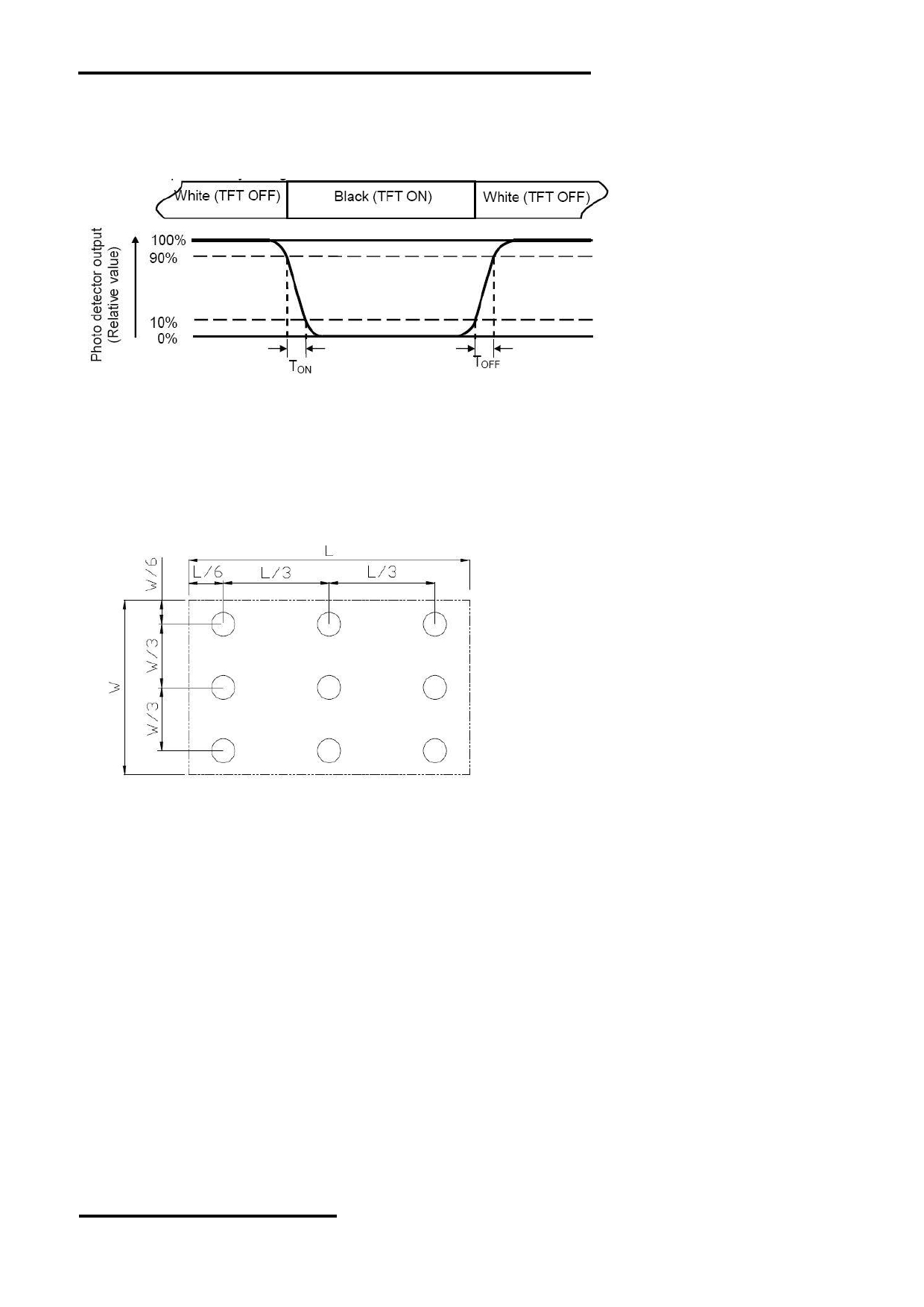
Note 4: Definition of Response time
The response time is defined as the LCD optical switching time interval between “White” state and
“Black” state. Rise time (T ON ) is the time between photo detector output intensity changed from 90%
to 10%. And fall time (T OFF ) is the time between photo detector output intensity changed from 10% to
90%.
Note 5: Definition of color chromaticity (CIE1931)
Color coordinates measured at center point of LCD.
Note 6: Definition of Luminance Uniformity
Active area is divided into 9 measuring areas (Refer Fig. 2). Every measuring point is placed at the
center of each measuring area.
Luminance Uniformity (U) = Lmin/ Lmax
L-------Active area length W----- Active area width
Lmax: The measured Maximum luminance of all measurement position.
Lmin: The measured Minimum luminance of all measurement position.
Note 7: Definition of Luminance:
Measure the luminance of white state at center point.
URL: www.topwaydisplay.com
Document Name: LMT070FNMFWA-NND-1-Manual-Rev0.2
Page: 11 of 12
TOPWAY
LCD Module User Manual
LMT070FNMFWA_NNA
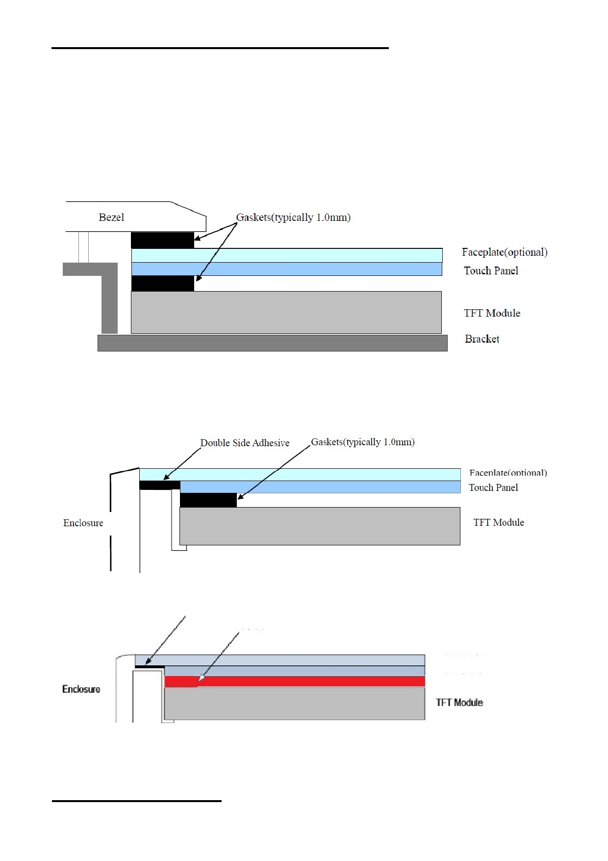
8. Touch panel Design Precautions
8.1 Mounting Precaution
9.1.1 Bezel Mounting
When mounting the CTP underneath a bezel,the CTP assembly should be mounted using a configuration
that supports the back surface of the TFT module.The bezel edge must be positioned outside the active area
of the CTP.A gap of 0.5mm to 1.0mm is needed between the bezel and the CTP surface.A foam gasket or
similar material should be used to compensate for the tolerance of the enclosure,compression for the
screw,etc.
9.1.2 Flush Mounting
When flush mounting the faceplate with the top of the enclosure,the enclosure must have a ledge for
attaching the overhang of the faceplate as well as a ledge for supporting the back of the TFT module.
9.1.3 Optical Bonding
When flush mounting the faceplate with the top of the enclosure,the enclosure must have a ledge for
attaching the overhang of the faceplate as well as a ledge for supporting the back of the TFT module.
9. Precautions of using LCD Modules
Please refer to "LCD-Module-Design-Handling-Precaution.pdf".
URL: www.topwaydisplay.com
Document Name: LMT070FNMFWA-NND-1-Manual-Rev0.2
Page: 12 of 12