LMT080DIEFWU-3
LCD Module User Manual
Prepared by:
Checked by:
Approved by:
Yu
Date: 2018-07-20
Date:
Date:
Rev. Descriptions
Release Date
0.1
Preliminary release
2017-07-10
0.2
Update section 6.1
2018-07-20
URL: www.topwaydisplay.com
Document Name: LMT080DIEFWU-3-Manual-Rev0.2
Page: 1 of 10

TOPWAY
LCD Module User Manual
LMT080DIEFWU-3
3
Table of Content
1. General Specification ............................................................................................................ 3
2. Block Diagram ........................................................................................................................ 3
3. Terminal Function .................................................................................................................. 4
3.1
K1 TFT Input Terminal ........................................................................................................................................... 4
3.2
K2 (Backlight connector) ........................................................................................................................................ 5
4. Absolute Maximum Ratings .................................................................................................. 5
5. Electrical Characteristics ...................................................................................................... 5
5.1
DC Characteristics ................................................................................................................................................. 5
5.2
Current Consumption ............................................................................................................................................. 5
5.3
LED Backlight Circuit Characteristics ..................................................................................................................... 5
5.4
Power on/off Sequence .......................................................................................................................................... 6
6. AC Characteristics ................................................................................................................. 7
6.1
Timing Characteristics ............................................................................................................................................ 7
6.2
Input Clock and Data Timing Diagram ................................................................................................................... 7
6.3
Recommended Timing Setting Of TCON ............................................................................................................... 8
6.4
Horizontal input timing Diagram ............................................................................................................................. 8
7. Optical Characteristics .......................................................................................................... 9
8. Precautions of using LCD Modules .................................................................................... 10
URL: www.topwaydisplay.com
Document Name: LMT080DIEFWU-3-Manual-Rev0.2
Page: 2 of 10

TOPWAY
LCD Module User Manual
LMT080DIEFWU-3
3
1. General Specification
Signal Interface :
Digital 24-bits RGB
Display Technology :
a-Si TFT active matrix
Display Mode :
Transmissive / Normal White
Screen Size(Diagonal) :
8.0”
Outline Dimension :
183.0 x 141.0 x 5.6 (mm)
(see attached drawing for details)
Active Area :
162.0 x 121.5 (mm)
Number of dots :
800 x 3 (RGB) x 600
Pixel Pitch :
0.2025 x 0.2025 (mm)
Pixel Configuration :
RGB Stripe
Backlight :
LEDs
Surface Treatment :
Anti-Glare Treatment
Viewing Direction :
6 o’clock(Gray scale Inversion) ( *1 )
12 o’clock (*2)
Operating Temperature :
-20 ~ +70°C
Storage Temperature :
-30 ~ +80°C
Note:
*1. For saturated color display content (eg. pure-red, pure-green, pure-blue or pure-colors -combinations).
*2. For “ color scales ” display content.
*3. Color tone may slightly change by temperature and driving condition.
2. Block Diagram
Backlight
BLA, BLK
800(x3) x 600 pixels
TFT Panel
R0~R7, B0~B7, G0~G7
DCLK, DE, VS, HS
Source Driver
MODE, RESET, DITHB
L/R, U/D
Vcc, GND, V COM, AV DD
V GL, V GH
Power Circuit
URL: www.topwaydisplay.com
Document Name: LMT080DIEFWU-3-Manual-Rev0.2
Page: 3 of 10
TOPWAY
LCD Module User Manual
LMT080DIEFWU-3
3
3. Terminal Function
3.1 K1 TFT Input Terminal
Pin No.
Pin Name
I/O
Descriptions
1
:
NC
-
No Connection
4
5
GND
Power
Power GND (0V)
6
V COM
Input
Common voltage
7
Vcc
Power
Power for Digital Circuit
8
MODE
Input
DE/SYNC mode select (*1)
9
DE
Input
Data input enable
10
VS
Input
Vertical Sync Input
11
HS
Input
Horizontal Sync Input
12
B7
:
:
Input
8bit Data for Blue
19
B0
20
G7
:
:
Input
8bit Data for Green
27
G0
28
R7
:
:
Input
8bit Data for Red
35
R0
36
GND
Power
Power GND (0V)
37
DCLK
Input
Sample clock(*2)
38
GND
Power
Power GND (0V)
39
L/R
Input
Left / right selection (*3)
40
U/D
Input
Up/down selection (*3)
41
V GH
Power
Gate ON Voltage
42
V GL
Power
Gate OFF Voltage
43
AV DD
Power
Power for Analog Circuit
44
RESET
Input
Global reset pin (*4)
45
NC
-
No connection
46
V COM
Input
Common Voltage
Dithering function
47
DITHB
Input
DITHB=0,Disable internal dithering function.
DITHB=1,Enable internal dithering function.
48
GND
Power
Power GND (0V)
49
NC
-
50
NC
No connection
Note:
* 1: When select DE mode, MODE=”1”.
When select SYNC mode, MODE= “0”.
* 2: Data shall be latched at the falling edge of DCLK.
* 3: Selection of scanning mode
Setting of scan control input
U/D
L/R
Scanning direction
GND
Vcc
Up to down, left to right
Vcc
GND
Down to up, right to left
GND
GND
Up to down, right to left
Vcc
Vcc
Down to up, left to right
*4: Global reset pin. Active low to enter reset state. Suggest to connect with an RC reset circuit for stability. Normally pull high.
URL: www.topwaydisplay.com
Document Name: LMT080DIEFWU-3-Manual-Rev0.2
Page: 4 of 10
TOPWAY
LCD Module User Manual
LMT080DIEFWU-3
3
3.2
K2 (Backlight connector)
Pin No. Pin Name
IO
Descriptions
Wire Color
1
BLA
Power
LED driving anode (high voltage)
Red
2
BLK
Power
LED driving cathode (low voltage)
White
4. Absolute Maximum Ratings
Items
Symbol
Min.
Max.
Unit
Condition
Vcc
-0.5
3.96
V
Power voltage
AV DD
-0.5
14.85
V
V GH
-0.3
+42
V
V GL
V GH -42
+0.3
V
Operating Temperature
T OP
-20
70
C
No Condensation
Storage Temperature
T ST
-30
80
C
No Condensation
Note:
*1. This rating applies to all parts of the module. And should not be exceeded.
*2. The operating temperature only guarantees operation of the circuit. The contrast, response speed,
and the other specification related to electro-optical display quality is determined at the room temperature, T OP =25.
*3. Ambient temperature when the backlight is lit (reference value)
*4. Any Stresses exceeding the Absolute Maximum Ratings may cause substantial damage to the device. Functional
operation of this device at other conditions beyond those listed in the specification is not implied and prolonged
exposure to extreme conditions may affect device reliability.
5. Electrical Characteristics
5.1 DC Characteristics
Items
Symbol
Min.
Typ.
Max.
Unit
Remark
Vcc
2.8
3.3
3.6
V
*2
Power voltage
AV DD
12.4
12.6
12.8
V
V GH
20
22
24
V
V GL
-7.4
-6.9
-6.4
V
Input signal voltage
V COM
4.05
4.1
4.15
V
Input logic high voltage
V IH
0.7Vcc
-
Vcc
V
Input logic low voltage
V IL
0
-
0.3Vcc
V
*3
Note:
*1.Be sure to apply VCC and VGL to the LCD first, and then apply VGH.
*2: VCC setting should match the signals output voltage (refer to Note 3) of customer’s system board.
*3: DCLK,HS,VS,RESET,U/D, L/R,DE,R0~R7,G0~G7,B0~B7,MODE,DITHB.
5.2 Current Consumption
Items
Symbol
Min.
Typ.
Max.
Unit
Remark
I GH
-
0.28
0.4
mA
V GH = 22.0V
Current for Driver
I GL
-
0.29
0.4
mA
V GL = -7.0V
I CC
-
3.10
10
mA
V DD =3.3V
I AV DD
-
17.8
28
mA
AV DD =12.5V
5.3 LED Backlight Circuit Characteristics
Top=25 ℃
Items
Symbol
MIN.
TYP.
MAX.
Unit
Note
Forward Voltage
Vf BLA
9.0
9.6
10.3
V
If=180mA
Forward Current
If BLA
-
180
225
mA
Backlight Life Time
-
20,000 25,000
-
hr
If=180mA
Note:
*1. Exceeding the recommended driving current could cause substantial damage to the backlight and shorten its lifetime.
URL: www.topwaydisplay.com
Document Name: LMT080DIEFWU-3-Manual-Rev0.2
Page: 5 of 10

TOPWAY
LCD Module User Manual
LMT080DIEFWU-3
3
5.4 Power on/off Sequence
Item
Symbol Min
Typ
Max
Unit
Remark
VCC 3.3V rising time
T1
0
-
20
ms
VCC to AVDD on time
T2
16.7
-
-
ms
AVDD to VGL on time
T3
0
-
-
ms
VGL to VGH on time
T4
0
-
-
ms
VGH to DATA on time
T5
0
-
-
ms
DATA to BL on time
T6
0
-
-
ms
Note:
*1. Power on sequence: VCC AVDD VGL VGH DATA ON BACKLIGHT ON
*2. Power off sequence: BACKLIGHT OFF DATA OFF VGH VGL AVDD VCC
*3. When VCC turned on, the rising time T1 should less than 20ms.
*4. AVDD stable to VCC stable time T2 should better longer than 1 frame time.
*5. The power off sequence can be set according to power on settings.
URL: www.topwaydisplay.com
Document Name: LMT080DIEFWU-3-Manual-Rev0.2
Page: 6 of 10
TOPWAY
LCD Module User Manual
LMT080DIEFWU-3
3
6. AC Characteristics
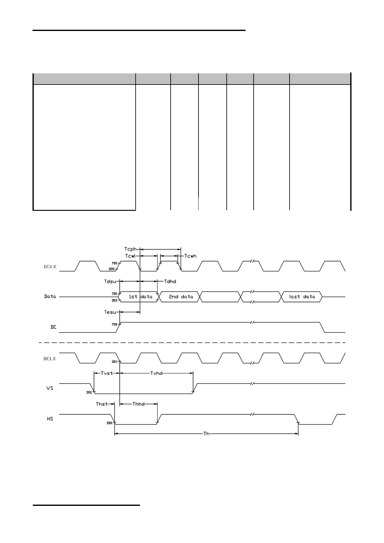
6.1 Timing Characteristics
Item
Symbol
MIN.
TYP.
MAX.
Unit
Remark
VDD Power On Slew rate
T POR
-
-
20
ms
From 0V to 90% VDD
DCLK Cycle Time
Tcph
14
-
-
ns
DCLK Pulse Width
Tcw
40
50
60
%
VSD Setup Time
Tvst
5
-
-
ns
VSD Hold Time
Tvhd
5
-
-
ns
HSD Setup Time
Thst
5
-
-
ns
HSD Hold Time
Thhd
5
-
-
ns
Data Setup Time
Tdsu
5
-
-
ns
Data to DCLK
Data Hold Time
Tdhd
5
-
-
ns
Data to DCLK
DE Setup Time
Tesu
5
-
-
ns
DE Hold Time
Tehd
5
-
-
ns
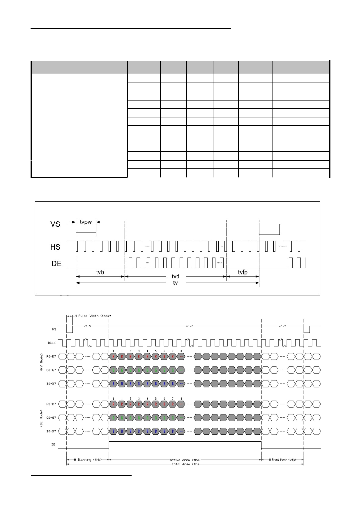
6.2 Input Clock and Data Timing Diagram
URL: www.topwaydisplay.com
Document Name: LMT080DIEFWU-3-Manual-Rev0.2
Page: 7 of 10
TOPWAY
LCD Module User Manual
LMT080DIEFWU-3
3
6.3 Recommended Timing Setting Of TCON
TCON (Embedded In Source IC) Input Timing (DCLK, HSD, VSD, DE)
VCC=3.3V, AVDD=12.6V, AGND=GND=0V, Ta=25 ℃
Item
Symbol
MIN.
TYP.
MAX.
Unit
Remark
F clk
34.5
39.6
50.4
MHZ
DCLK
t clk
-
25.3
-
ns
t h
900
1000
1200
t clk
t hd
-
800
-
t clk
HSD
t hpw
1
-
40
t clk
t hb
-
88
-
t clk
t hfp
12
112
312
t clk
t v
640
660
700
t h
t vd
-
600
-
t h
VSD
t vpw
1
-
20
t h
t vb
-
39
-
t h
t vfp
1
21
61
t h
Note: DE timing refer to HSD, VSD input timing.
Vertical input timing Diagram:
6.4 Horizontal input timing Diagram
Horizontal input timing diagram
URL: www.topwaydisplay.com
Document Name: LMT080DIEFWU-3-Manual-Rev0.2
Page: 8 of 10
TOPWAY
LCD Module User Manual
LMT080DIEFWU-3
3
7. Optical Characteristics
Ta=25 ℃
Item
Symbol
Condition
MIN.
TYP.
MAX.
UNIT
Note.
θ L
9 o’clock
60
70
-
Viewing angle
θ R
3 o’clock
60
70
-
(CR ≥ 10)
degree
* 2
θ T
12 o’clock
50
60
-
θ B
6 o’clock
60
70
-
T f
msec
Response Time
25 ℃
-
25
30
* 1
T r
msec
* 4
Contrast ratio
CR
θ=0 o
600
800
-
-
*1,*3
X
0.253
0.303
0.353
White
Y
0.257
0.307
0.357
X
0.525
0.575
0.625
Red
Color
Y
Backlight 0.296 0.346
0.396
* 1
chromaticlty
X
is on
0.298
0.348
0.398
* 5
Green
Y
0.527
0.577
0.627
X
0.101
0.151
0.201
Blue
Y
0.031
0.081
0.131
Luminance
L
200
250
-
cd/m 2
* 1,*6
NTSC
45
50
-
%
* 5
Luminance uniformity
Y U
70
75
-
%
*1,*7
Note :
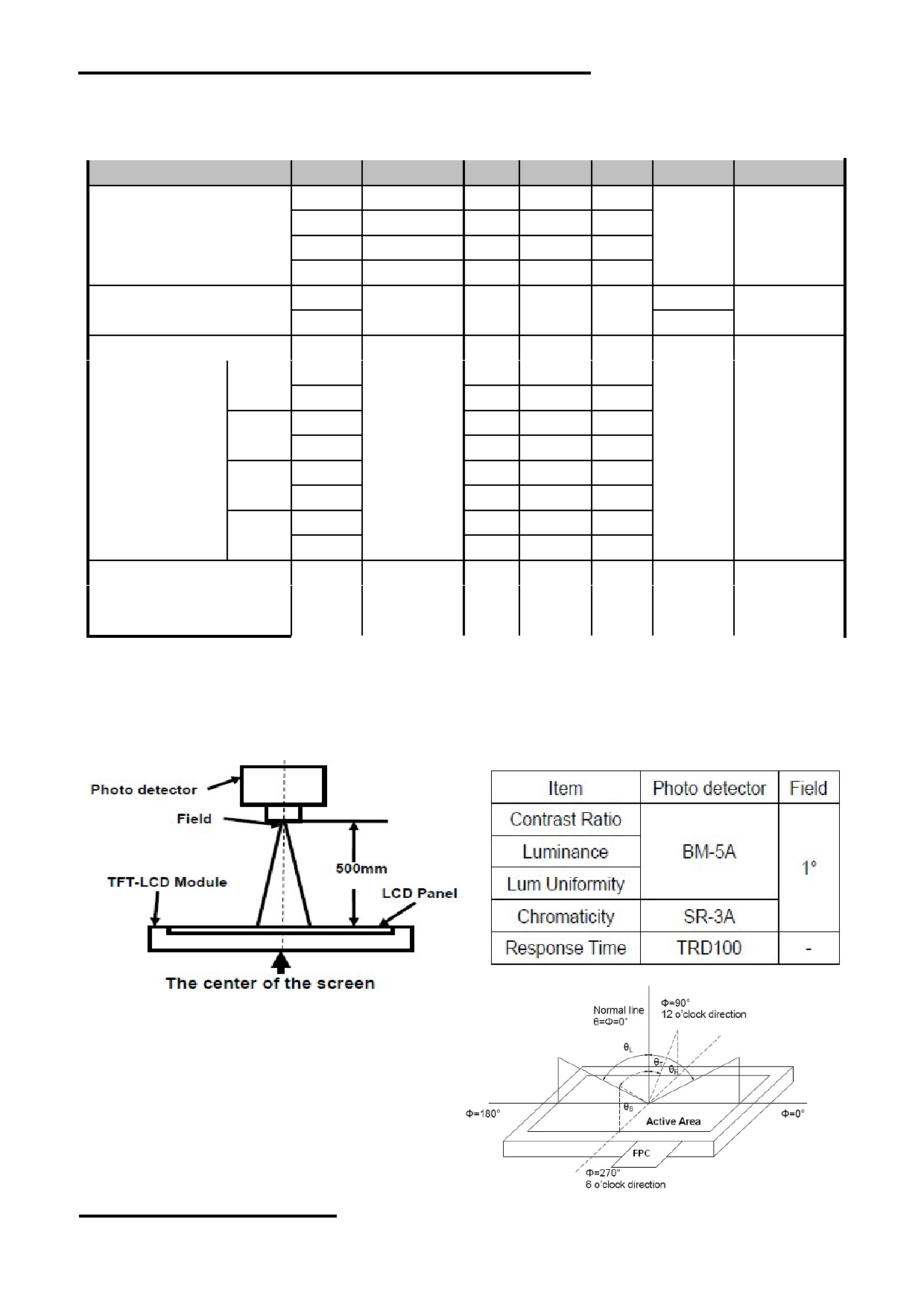
* 1: Definition of optical measurement system.
The optical characteristics should be measured in dark room. After 5 Minutes operation, the optical
properties are measured at the center point of the LCD screen. All input terminals LCD panel must
be ground when measuring the center area of the panel.
* 2: Definition of viewing angle range
URL: www.topwaydisplay.com
Document Name: LMT080DIEFWU-3-Manual-Rev0.2
Page: 9 of 10
TOPWAY
LCD Module User Manual
LMT080DIEFWU-3
3
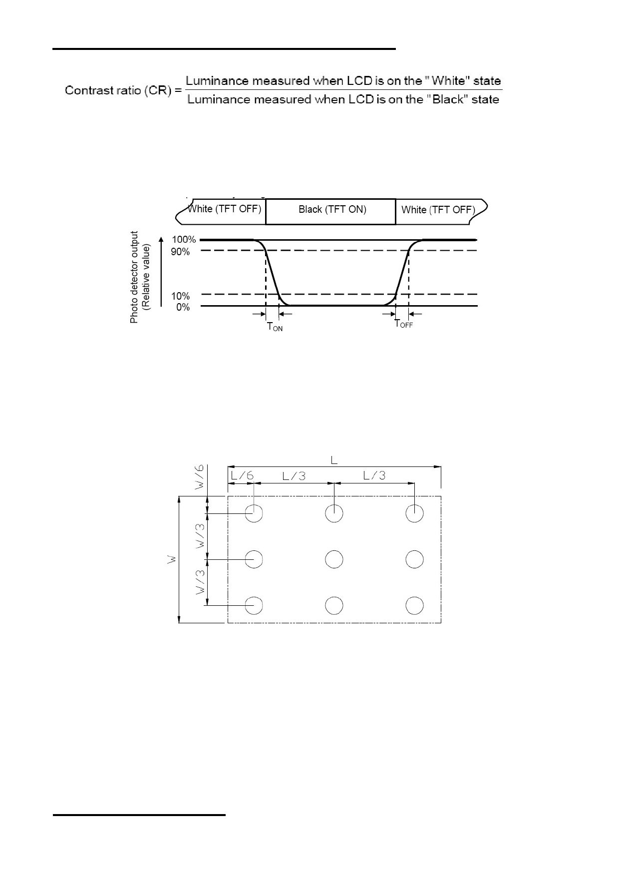
*3: Definition of contrast ratio
*4: Definition of Response time
The response time is defined as the LCD optical switching time interval between “ White ” state
and
“ Black ” state. Rise time (T ON ) is the time between photo detector output intensity changed from
90% to 10%. And fall time (T OFF ) is the time between photo detector output intensity changed from
10% to 90%.
* 5: Definition of color chromaticity (CIE1931)
Color coordinates measured at center point of LCD.
* 6: Definition of Luminance Uniformity
Active area is divided into 9 measuring areas (Refer Fig. 2). Every measuring point is placed at the
center of each measuring area.
Luminance Uniformity (U) = Lmin/ Lmax
L-------Active area length W----- Active area width
Lmax: The measured Maximum luminance of all measurement position.
Lmin: The measured Minimum luminance of all measurement position.
Note 7: Definition of Luminance:
Measure the luminance of white state at center point.
8. Precautions of using LCD Modules
Please refer to "LCD-Module-Design-Handling-Precaution.pdf".
URL: www.topwaydisplay.com
Document Name: LMT080DIEFWU-3-Manual-Rev0.2
Page: 10 of 10