LMT080ENPFSA
LCD Module User Manual
Prepared by:
Checked by:
Approved by:
Zhangwenbo
Date: 2026-03-13
Date:
Date:
Rev. Descriptions
Edit
Release Date
0.1
Preliminary release
Zhangwenbo
2026-03-13

CONTENTS
1. FEATURES ......................................................................................................................................................... 1
2. GENERAL SPECIFICATIONS .......................................................................................................................... 1
3. INPUT / OUTPUT TERMINALS..................................................................................................................... 2
3.1 CN1 Pin assignment (LCD Interface) ..................................................................................................................................................... 2
3.2 CN2 Pin assignment (Back Light) ............................................................................................................................................................ 3
4. ABSOLUTE MAXIMUM RATINGS ............................................................................................................... 4
5. ELECTRICAL CHARACTERISTICS ................................................................................................................. 5
5.1 DC Characteristics for Panel Driving ...................................................................................................................................................... 5
5.2 DC Characteristics for Backlight Driving ............................................................................................................................................... 6
5.3 Recommended Power ON/OFF Sequence .......................................................................................................................................... 7
5.4 LCD Module Block Diagram ..................................................................................................................................................................... 8
6. INTERFACE TIMING CHARACTERISTICS ................................................................................................... 9
6.1 LVDS AC characteristics .......................................................................................................................................................................... 9
6.2 DE Mode Data Input Timing Parameter Setting.............................................................................................................................. 11
6.3 LVDS signal format .................................................................................................................................................................................... 12
7. OPTICAL CHARACTERISTICS ..................................................................................................................... 13
8. MECHANICAL DRAWING ........................................................................................................................... 16
i
1.
Features
1.1 General Description
This is an 8.0 inch Amorphous-TFT-LCD (Thin Film Transistor Liquid Crystal Display) Normally
Black technology module, which is composed of a TFT-LCD panel, LCD Driver IC , FPC and a
LED backlight unit. It is designed for Automotive and other high reliability electronic products and
complies with the RoHS environmental protection directive.
1.2 Features
(2015/863/EU,Amending Annex II of 2011/65/EU)
2.
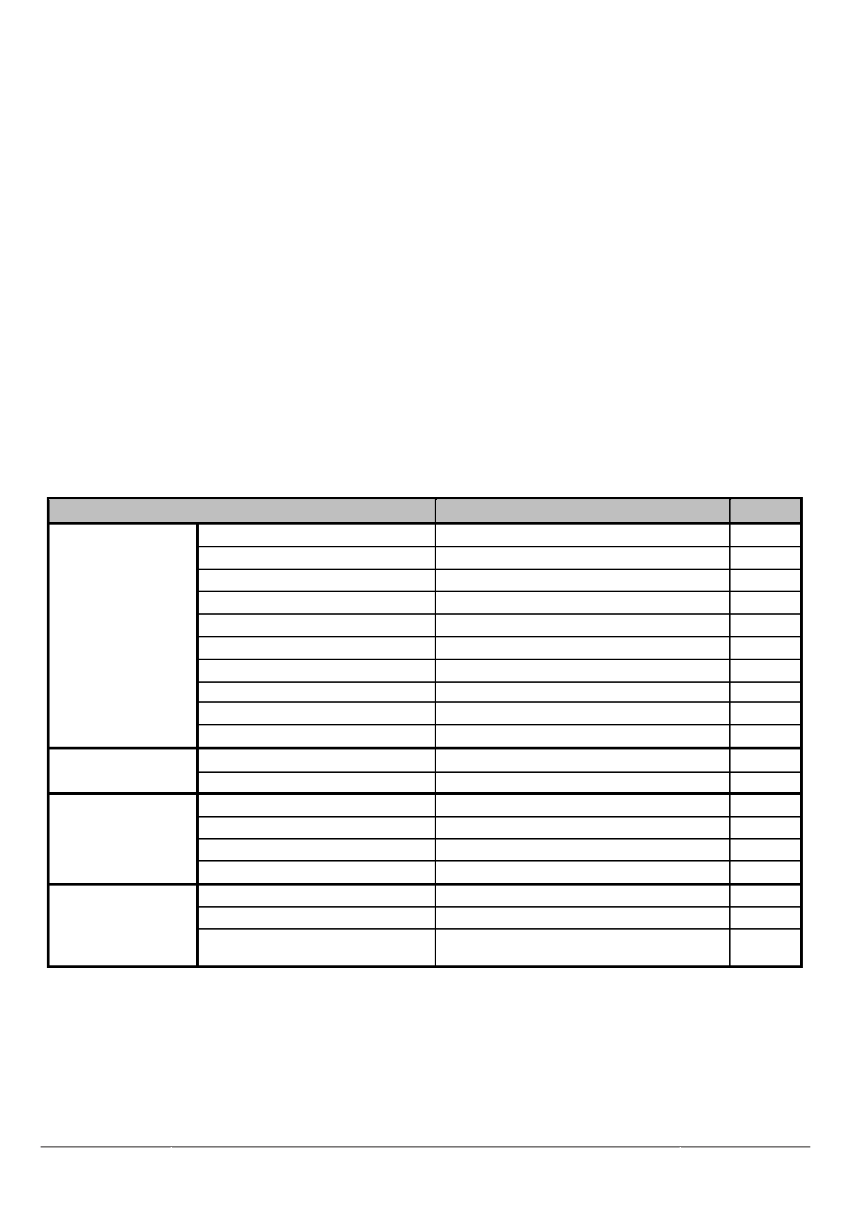
General Specifications
Feature
Spec
Unit
Size
8.0 inch
Resolution
1280(RGB)x720
Pixel Pitch
0.138 x 0.138
mm
TFT Active Area
176.64 x 99.36
mm
Display Spec
Technology Type
a-Si
Pixel Configuration
R.G.B Vertical Stripe
Display Mode
Normally Black SFT technology
Surface Treatment
HC
Viewing Direction
All
Gray Scale Inversion Direction
No gray inversion.
Mechanical
LCM (W x H x D)
192.8x116.9x6.4
mm
Characteristics
Weight
186 ± 5%
g
Luminance
Min : 850
Typ : 1200
cd/m 2
Optical
Contrast Ratio
Min: 900:1 Typ:1300:1
Characteristics
NTSC
Typ:73
%
Viewing Angle
88/88/88/88
degree
Interface
LVDS
Electrical
Color Depth
16.7 Million
color
Characteristics
Power Consumption
LCD:1.0725
Backlinght:6.588
W
Table 2.1 General TFT Specifications
Note 1: Requirements on Environmental Protection: Q/S0002 .
Note 2: The height dimension does not include the length of FPC.
Note 3: LCM weight tolerance: ±5%.
1
3.
Input / Output Terminals
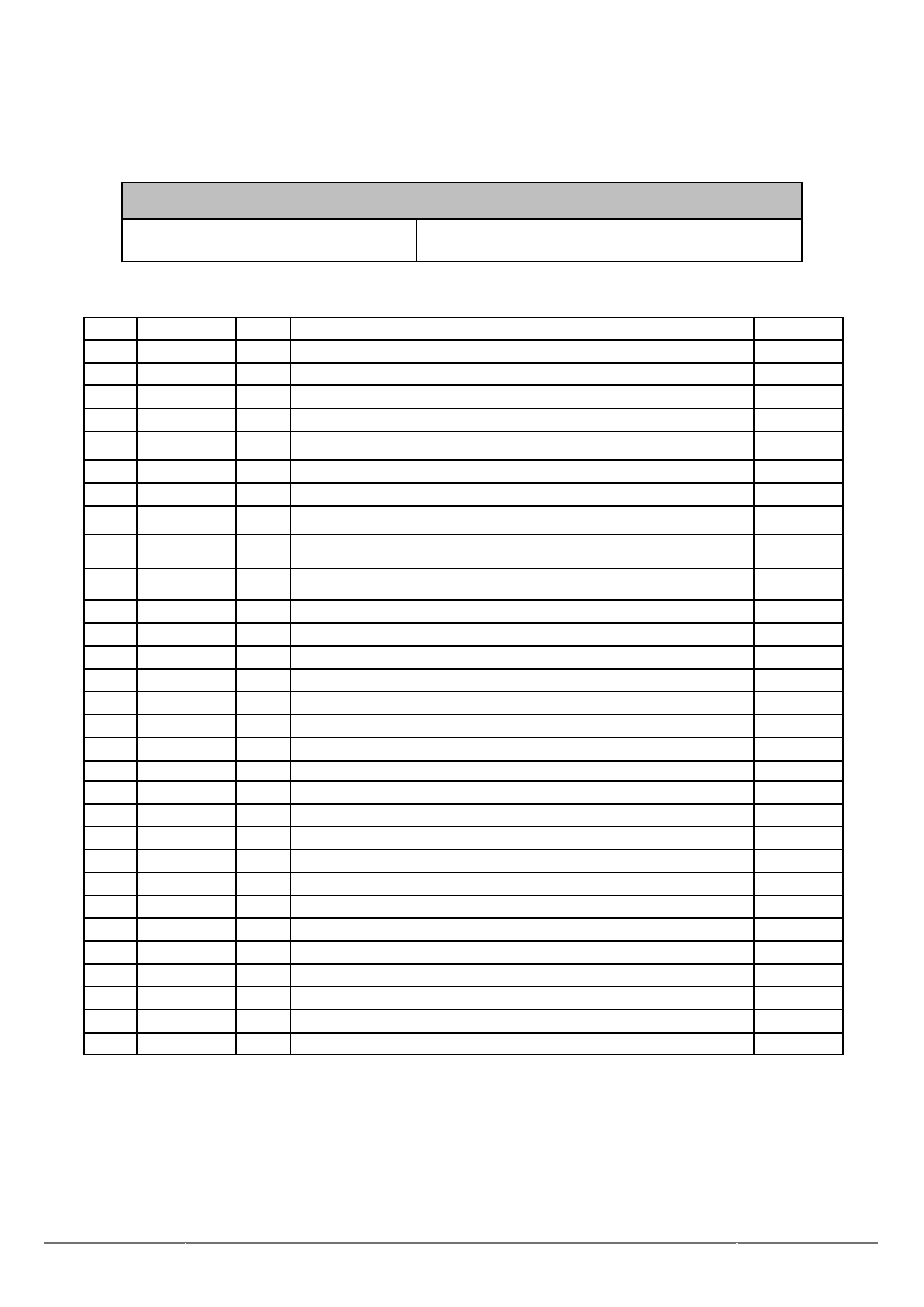
3.1 CN1 Pin assignment (LCD Interface)
C onnector Information
Mat ch ing connector
FH28D - 30S - 0.5SH (H irose )
Table 3.1.1 Connector information
No
Symbol
I/O
Description
Remark
1
NC
N
Keep this pin open .
2
VDD
P
Power supply 3.3V(Typ)
3
VDD
P
Power supply 3.3V(Typ)
4
GND
P
Power Ground
5
RESET
I
R eset signal
6
STBYB
I
Standby mode control signal
7
GND
P
Power Ground
8
SDA
N
Only for Tianma OTP use, Keep this pin open
9
SCL
N
Only for Tianma OTP use, Keep this pin open
10
CSB
N
Only for Tianma OTP use, Keep this pin open
11
GND
P
Power Ground
12
UD
I
Vertical shift direction selection
13
RL
I
Horizontal shift direction selection
14
GND
P
Power Grou nd
15
LV0N
I
Negative LVDS Differential data input(0)
16
LV0P
I
Positive LVDS Differential data input(0)
17
GND
P
Power Ground
18
LV1N
I
Negative LVDS Differential data input(1 )
19
LV1P
I
Negative LVDS Differential data input(1 )
20
GND
P
Pow er Ground
21
LV2N
I
Negative LVDS Differential data input(2 )
22
LV2P
I
Positive LVDS Differential data input(2 )
23
GND
P
Power Ground
24
CLKN
I
Negative LVDS Differential clock input
25
CLKP
I
Positive LVDS Differential clock input
26
GND
P
Power Ground
27
LV3N
I
Negative LVDS Differential data input(3 )
28
LV3P
I
Positive LVDS Differential data input(3 )
29
GND
P
Power Ground
30
VDDOTP
N
Power input for OTP programming, Keep this pin
open
Table 3.1.2 Pin Assignment for LCD Interface
Note1: I/O definition: I---Input, O---Output, P---Power/Ground, N---No connection
Note2: All of the GND pins should be connected to the system ground.
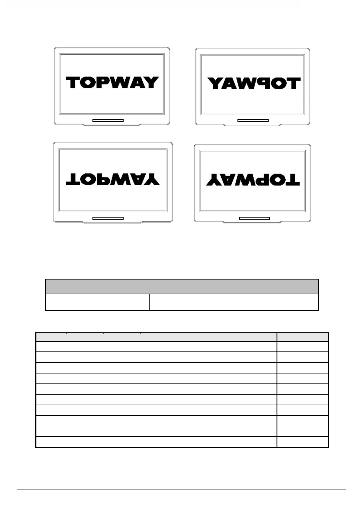
Note3: Description of Scan Direction.
2
RL=H, UD=H
RL=L, UD=H
RL=H, UD=L
RL=L, UD=L
Figure 3.1.1 Description of Scan Direction
3.2 CN2 Pin assignment (Back Light)
Connector Information
Matching connector
FH28-10S-0.5SH Hirose
Table 3.2.1 Connector information
No
Symbol
I/O
Description
Remark
1
A1
P
LED Anode
2
A2
P
LED Anode
3
A3
P
LED Anode
4
NC
N
Keep this pin open
5
THER+
I/O
Thermistor +
6
THER-
I/O
Thermistor -
7
NC
N
Keep this pin open
8
C3
P
LED Cathode
9
C2
P
LED Cathode
10
C1
P
LED Cathode
Table 3.2.1 Pin Assignment for Back Light Interface
Note1: I/O definition: I---Input, O---Output, P---Power/Ground, N---No connection
Note2: All of the GND pins should be connected to the system ground.
3
4. Absolute Maximum Ratings
Item
Symbol
MIN
MAX
Unit
Remark
Power Voltage
VDD
-0.3
5.0
V
Note1
Operating Temperature
Top
-30
85
℃
Storage Temperature
Tst
-40
85
℃
--
≤95
%
Ta≤40 ℃
--
≤85
%
40 ℃< Ta≤50 ℃
Relative Humidity
Note2
RH
--
≤55
%
50 ℃< Ta≤60 ℃
--
≤36
%
60 ℃< Ta≤70 ℃
--
≤24
%
70 ℃< Ta≤80 ℃
Absolute Humidity
AH
--
≤70
g/m³
Ta > 70 ℃
Table 4.1 Absolute Maximum Rating
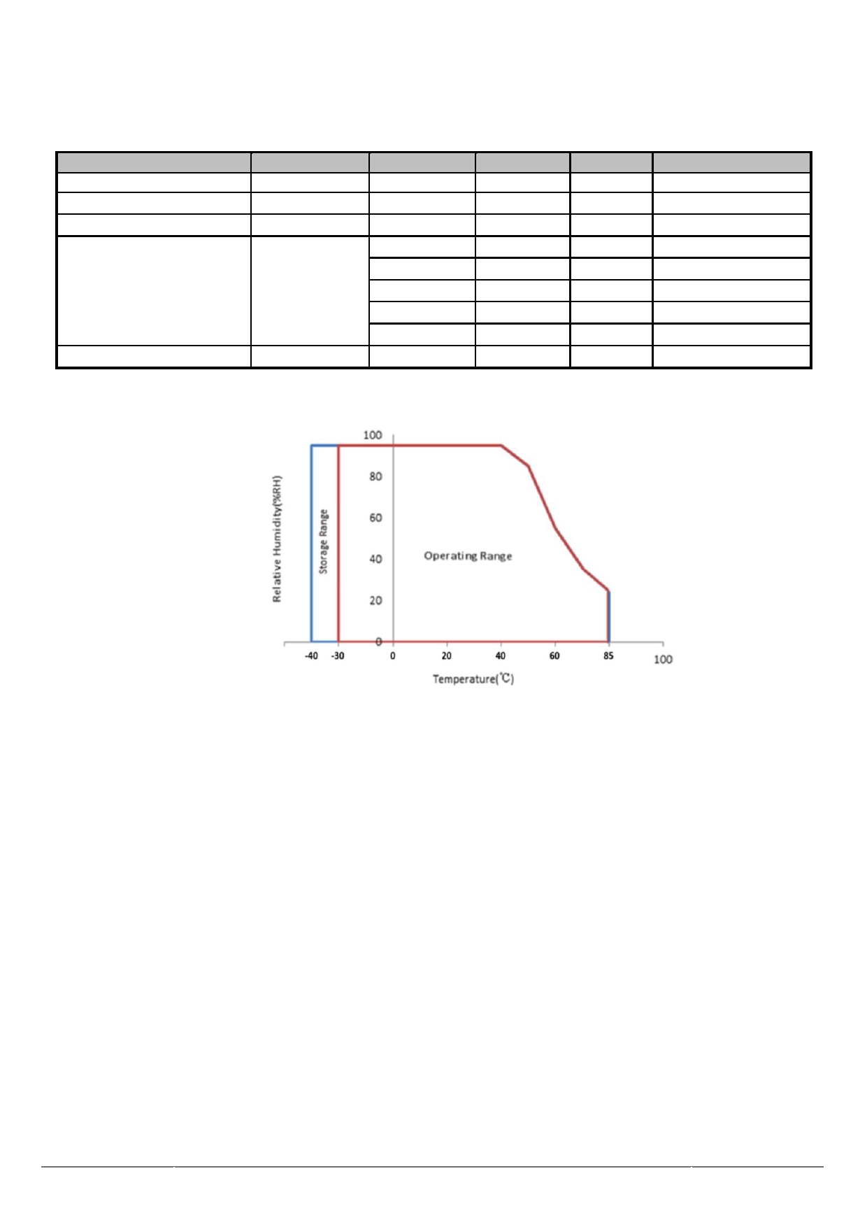
Figure 4.1 Absolute Maximum Ratings chart
Note1: Ta means the ambient temperature. It is necessary to limit the relative humidity to the specified
temperature range. Condensation on the module is not allowed.
Note2: The absolute maximum rating values of this product are not allowed to be exceeded at any times. A
module should be used with any of the absolute maximum ratings exceeded, the characteristics of the
module may not be recovered, or in an extreme condition, the module may be permanently destroyed
4
5.
Electrical Characteristics
5.1 DC Characteristics for Panel Driving
GND=0V, Ta = 25 ℃
Item
Symbol
MIN
TYP
MAX
Unit
Remar
k
Logic supply voltage
VDD
3.0
3.3
3.6
V
VDD Current
Ivdd
-
325
-
mA
Permissible Ripple Voltage of VDD
Vr
100
mV
Input High Voltage
V IH
0.7*VDD
VDD
V
Input Low Voltage
V IL
GND
0.3*VDD
V
Note 1
Differential Input common Mode
voltage
RXVCM
1
1.2
1.4
V
(1.5-
Differential Input voltage
|VID|
0.1
-
RxVCM)*
V
Note 2
2
Differential Input leakage Current
RVXliz
-10
-
10
uA
VDD Inrush current
Irush
-
-
1.5
A
Note3
Table 5.1.1 Operating Voltages
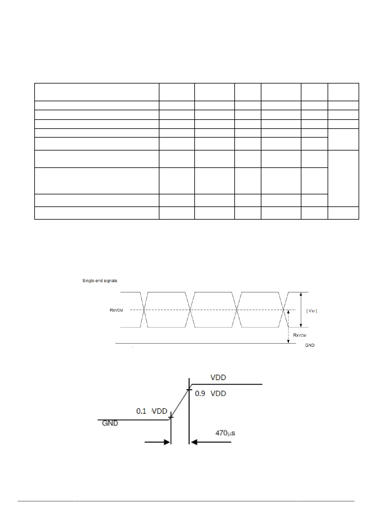
Note1: RESET, STBYB, RL, UD.
Note2: LVDS input signal electrical characteristics
Note3: Test condition of VDD Inrush current: The rise time of 10%VDD to 90%VDD is 470us.
Fig 5.1.1 LVDS mode DC electrical characteristics
Figure 5.1.2 VDD Inrush current
5
5.2 DC Characteristics for Backlight Driving
Item
Symbol
Min
Typ
Max
Unit
Remark
Forward Current
I BL
-
120
-
mA
Note1
Forward Voltage
V BL
16.8
18.3
20.4
V
Note2
Backlight
Power
Consumption
V BL
-
6.588
-
W
Note2
Lifetime
-
30000
50000
-
Hrs
Note3
Table 5.2.1 LED Backlight Characteristics
Note1: I is defined for each channel.
F
Note2: Optical performance should be evaluated at Ta=25 ℃ only.
Note3: If LED is driven by high current, high ambient temperature & humidity condition,The life time of LED will
be reduced.
Note4: Operating life means brightness goes down to 50% of initial brightness. Typical operating life time is
estimated data.
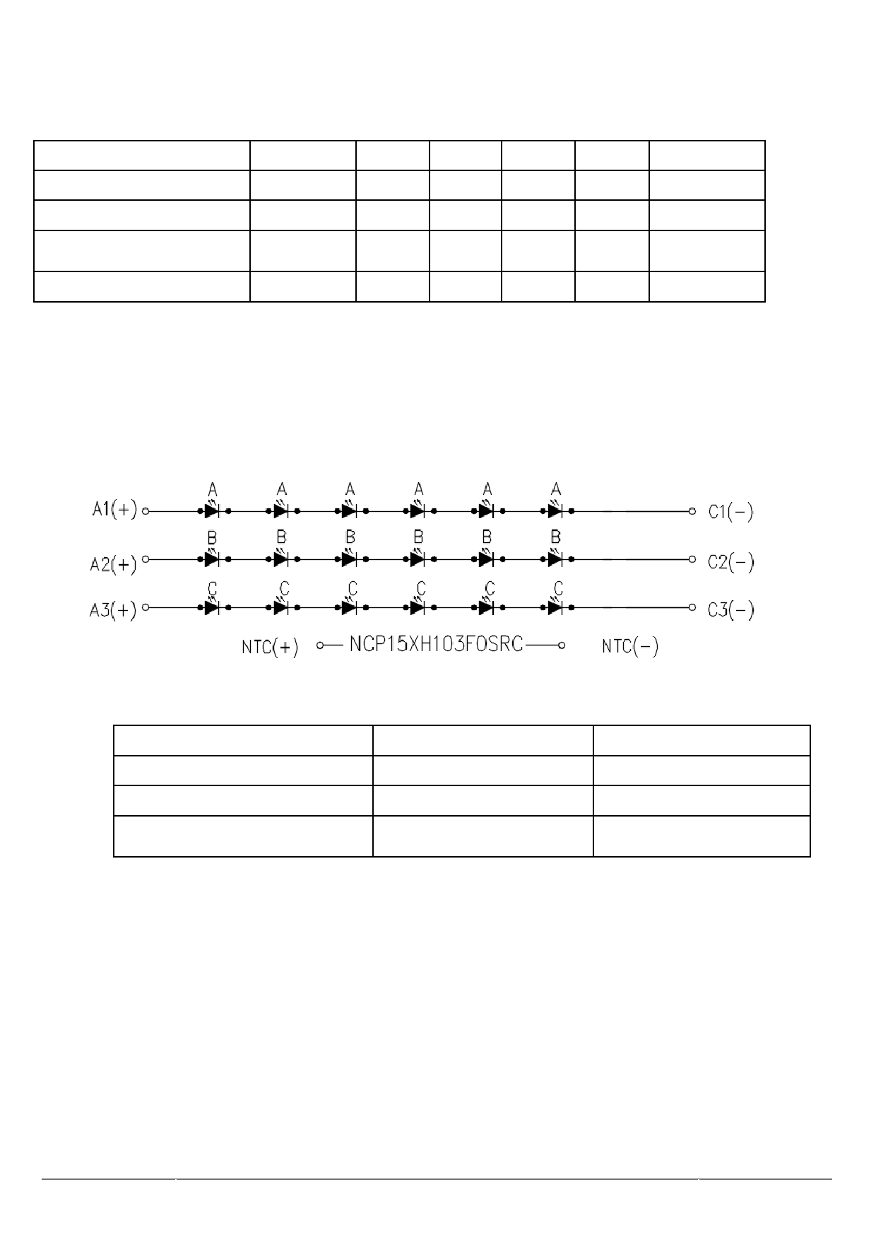
Figure 5.2.1 LED connection of backlight
Item
Value
Remarks
Part Number
NCP15XH103F0SRC
Murata
Resistance / Tolerance
10kΩ±1%
Ta=25 ℃
Permissive Operating Current
0.31mA
Ta=25°C
Note5
Table 5.2.2 Thermistor Description
Note1: I F is defined for one channel LEDs. There are a total of 3 LED channels in the backlight unit.
While the LCM is operating, a stable forward current should be supplied. The PWM value is
only for inrush current.
Note2: I F =120mA.
Note3: Optical performance should be evaluated at Ta=25 ℃ only. If the LEDs are driven at high
current or at high ambient temperature & high humidity environment, the lifetime of the LEDs
will be reduced. Operating lifetime means the brightness will decrease to 80% of the original
brightness.
Note4: An NTC thermistor is included in the LED circuit. Part number: NCP15XH103F0SRC. It is
used for the measuring LED temperature and is located in the LED circuit on the backlight
FPC.
Note5: To reduce the influence of NTC self-heating and improve the measurement accuracy. suggest
6
the operating current of NTC be xx mA
Note6: When operating at high temperature, NTC resistance should not be below xx k Ώ
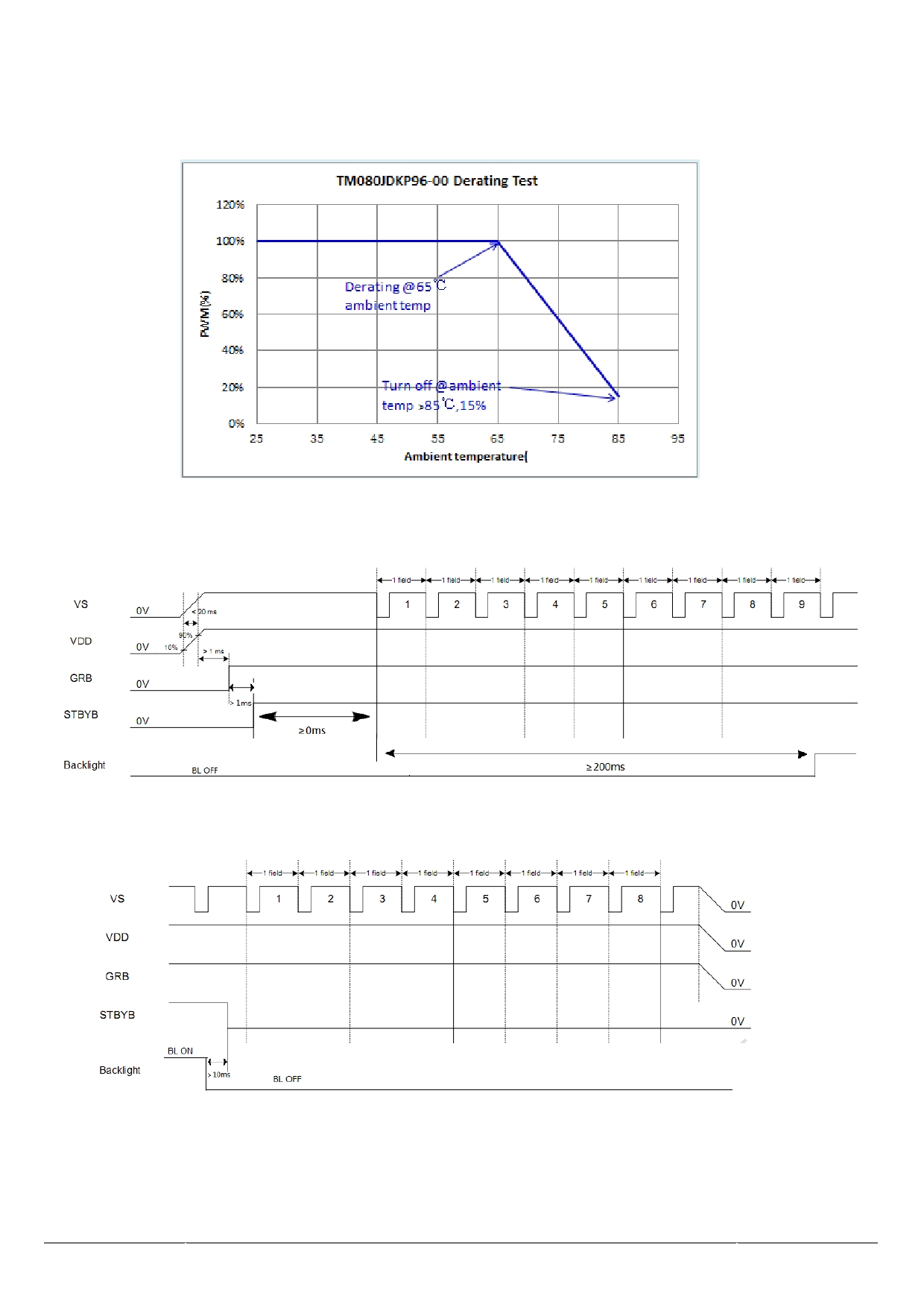
Figure 5.2.2 PWM vs Ambient Temperature
5.3 Recommended Power ON/OFF Sequence
Figure 5.3.1 Power on Sequence
Figure 5.3.2 Power off Sequence
Note1: GRB=RESET.
Note2: Power on/off of UD(RL) is at the same time as VDD.
7
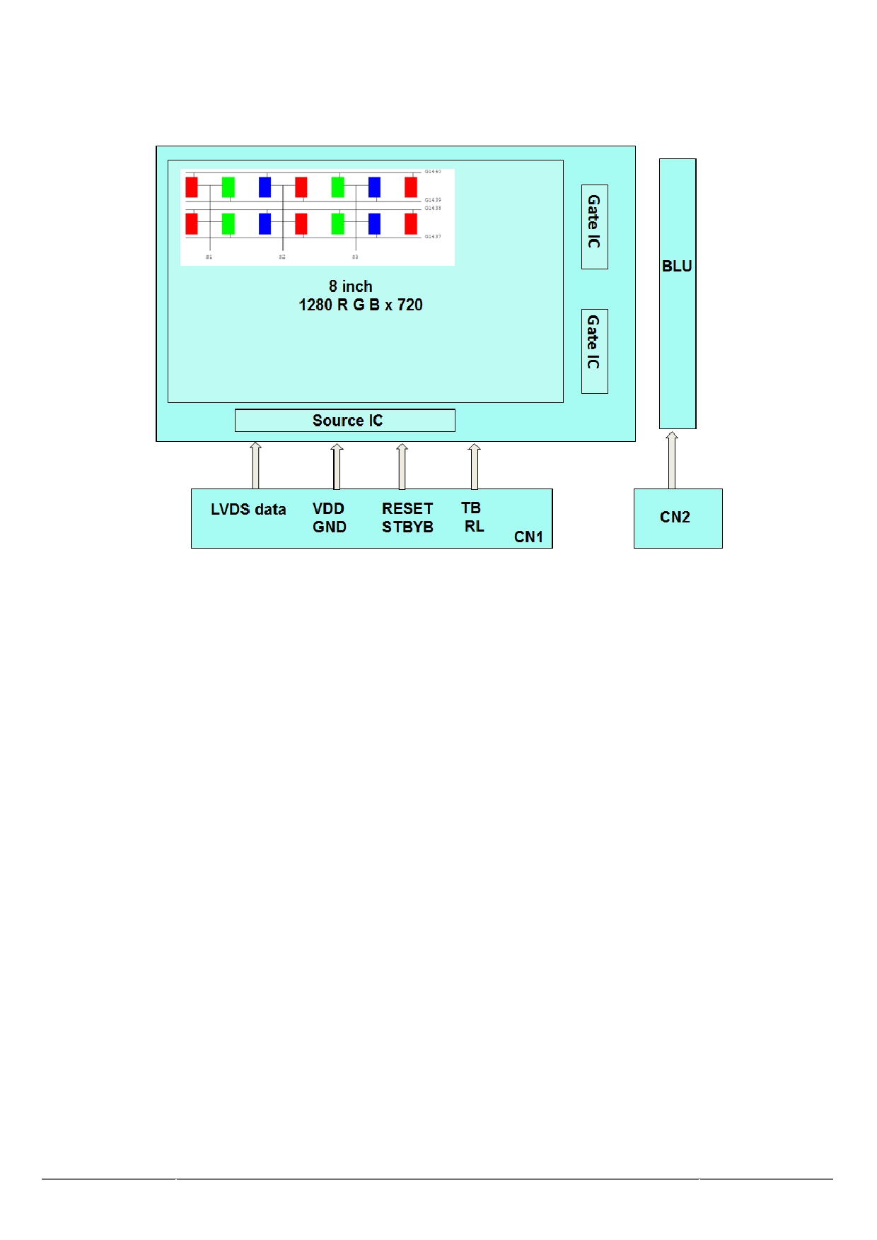
5.4 LCD Module Block Diagram
Figure 5.4.1 LCD Module Block Diagram
8
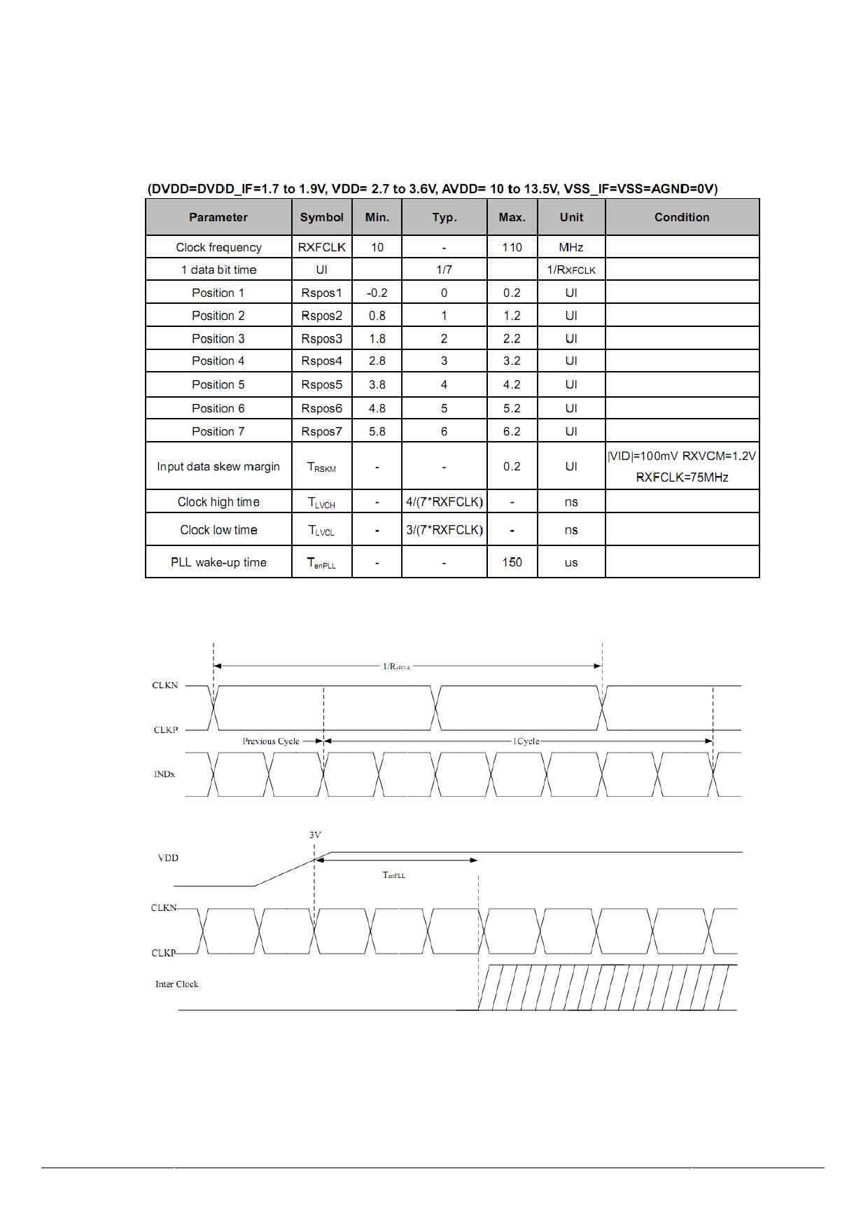
6.
Interface Timing Characteristics
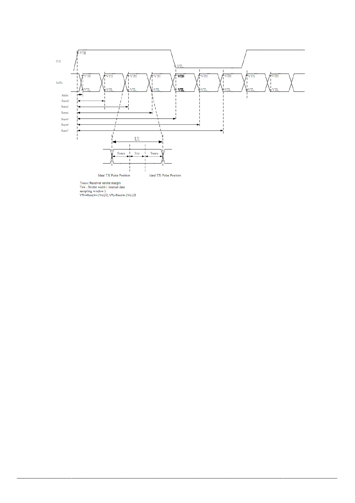
6.1 LVDS AC characteristics
Table 6.1.1 LVDS mode AC electrical characteristics
9
10
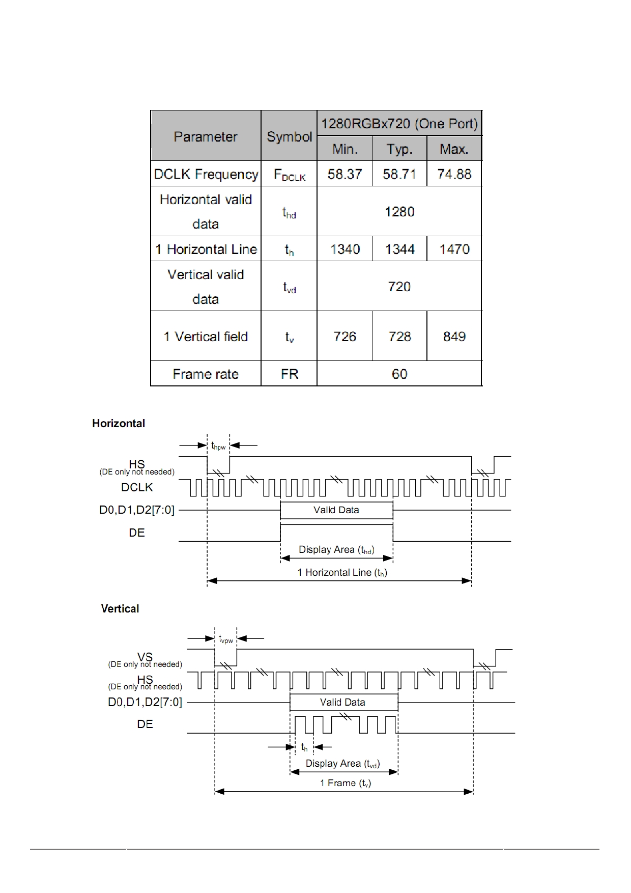
6.2 DE Mode Data Input Timing Parameter Setting
Table 6.2.1 Data Input Timing Parameters
Note : Above of all these information is just for reference , the final information should be based on
the test result of module and be set for module in initial code.
11
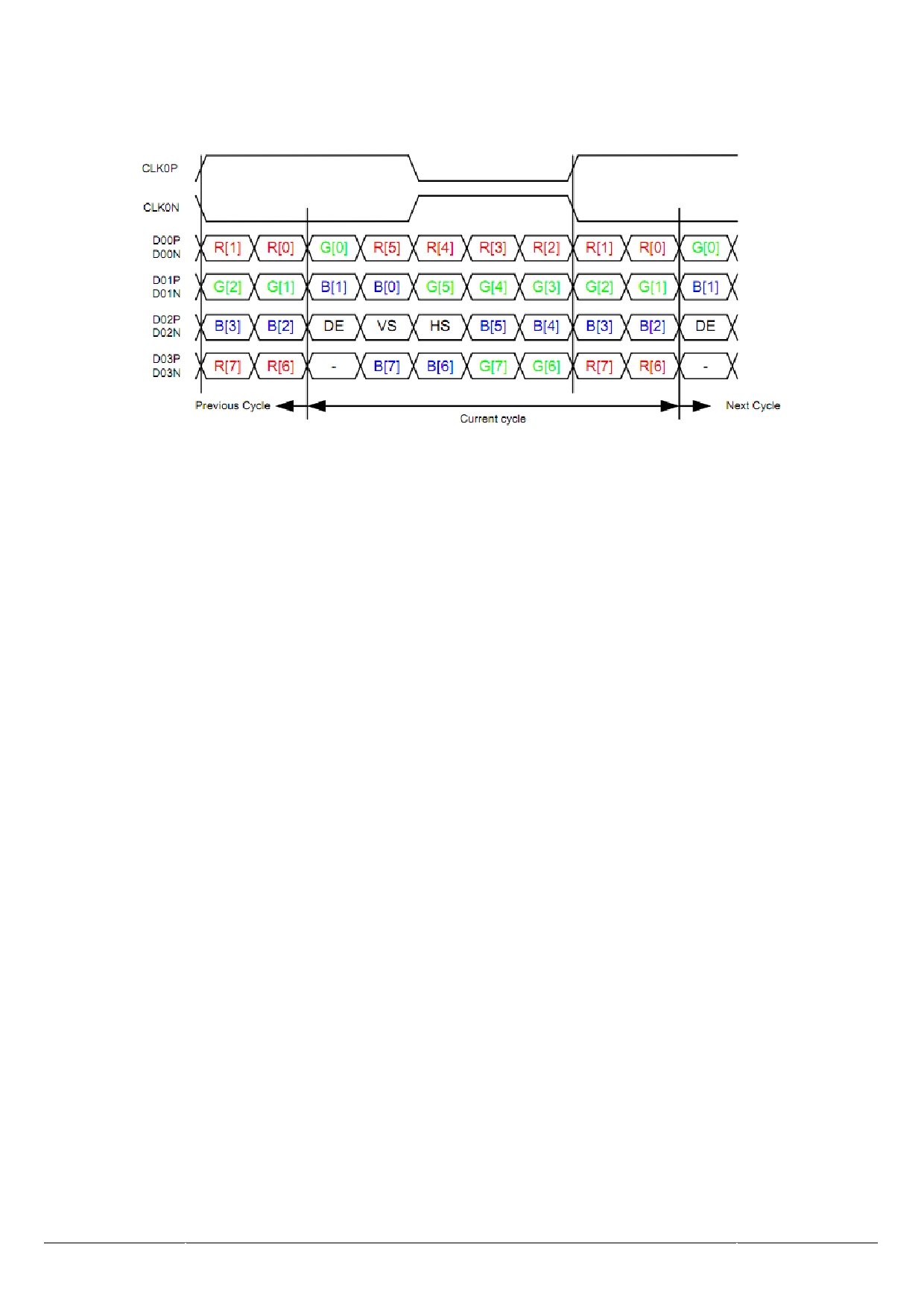
6.3 LVDS signal format
Figure 6.3.1 LVDS signals, VESA format
Note: CLK0P/N=CLKP/N, D00P/N=LV0P/N, D01P/N=LV1P/N, D02P/N=LV2P/N, D03P/N=LV3P/N
12
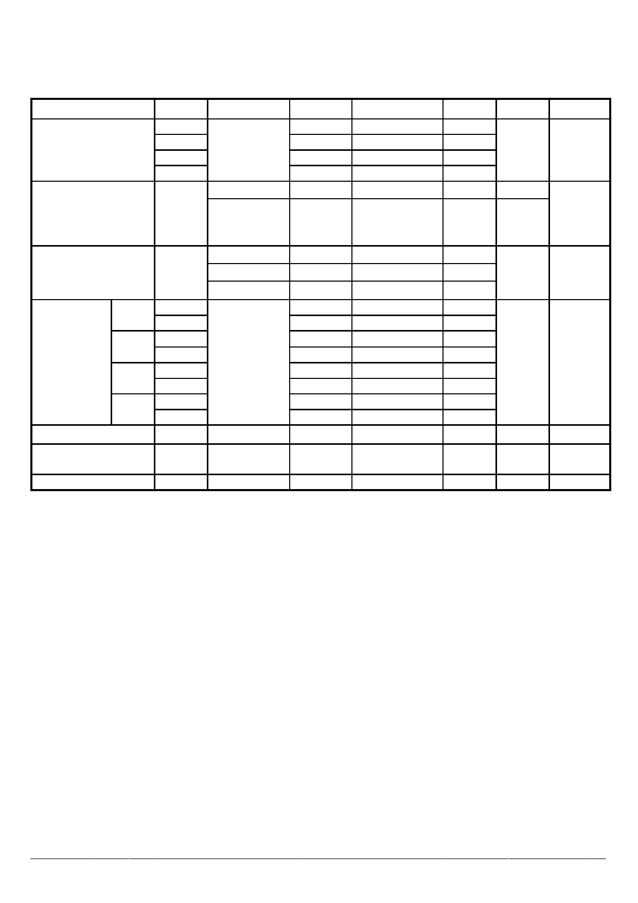
7. Optical Characteristics
Item
Symbol Condition
Min
Typ
Max
Unit
Remark
θ U
80
88
--
θ D
80
88
--
View Angles
Note1
θL
CR≥10
80
88
--
Degree
Note2
θR
80
88
--
Vertical,25 ℃ 900:1
1300:1
--
--
Contrast Ratio
CR
50%
Note3
Vertical,85 ℃ value of
--
--
--
Note6
25 ℃
25 ℃
--
--
25
Response Time
T ON +T OFF
-20 ℃
--
--
200
ms
Note4
-30 ℃
--
--
350
x
0.250
0.300
0.350
White
y
0.265
0.315
0.365
x
0.586
0.636
0.686
Red
Chromaticity
y
Backlight
0.286
0.336
0.386
is on
Note5
Green
x
0.256
0.306
0.356
y
0.579
0.629
0.679
x
0.095
0.148
0.195
Blue
y
0.013
0.063
0.113
Uniformity
White
--
75
80
--
%
Note7
NTSC
CIE1931-
XYZ
70
73
--
%
Note5
Luminance
L
--
850
1200
--
cd/m 2
Note8
Table 7.1 Optical Parameters
Test Conditions:
1. I F = 120 mA, and the ambient temperature is 25 ℃ .
2. The test systems refer to Note1 and Note2.
13
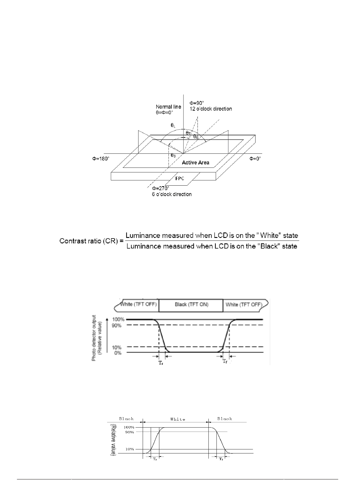
Note1: Definition of optical measurement system.
The optical characteristics should be measured in dark room. After 5 Minutes operation, the optical
characteristics are measured at the center point of the LCD screen.
Note2: Definition of viewing angle range and measurement system. Viewing angle is measured at the center
point of the LCD 。
Fig1. Measurement viewing angle
Note3: Definition of contrast ratio
Note4: Definition of Response time
For TN LCM,t he response time is defined as the LCD optical switching time interval between “White”
state and “Black” state. Rise time (T r ) is the time between photo detector output intensity changed from
90% to 10%. And fall time (T f ) is the time between photo detector output intensity changed from 10% to
90%.
Fig2. Response Time Testing(TN)
For SFT LCM, t he response time is defined as the LCD optical switching time interval between “White” state
and “Black” state. Rise time (T r ) is the time between photo detector output intensity changed from 10% to 90%.
And fall time (T f ) is the time between photo detector output intensity changed from 90% to 10%.
Fig3.Response Time Testing(SFT)
.
14
Note5: Definition of color chromaticity (CIE1931)
Color coordinates measured at center point of LCD.
Note 6: Contrast ratio against temperature
CR defines the allowed contrast reduction at the defined temperature based on the CR at room
temperature. For example: CR = (CR@25°C – CR@85°C) / CR@25°C x 100%
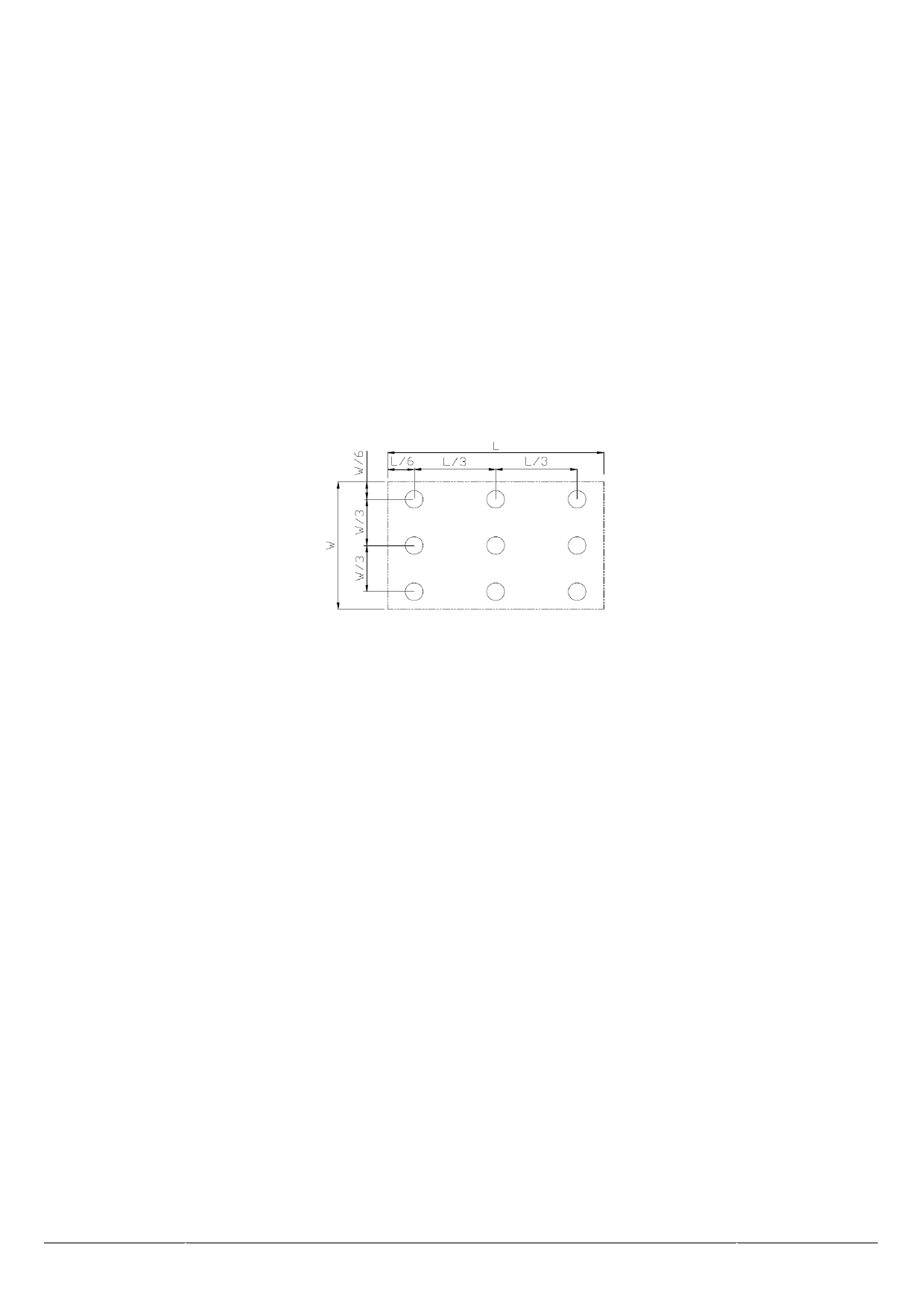
Note7: Definition of Luminance Uniformity
Active area is divided into 9 measuring areas (Refer Fig.4). Every measuring point is placed at the
center of each measuring area.
Luminance Uniformity (U) = Lmin/ Lmax
Lmax: The measured Maximum luminance of all measurement position.
Lmin: The measured Minimum luminance of all measurement position.
L-------Active area length; W----- Active area width
Fig4. Luminance Uniformity Measurement Locations(9 points)
Note8: Definition of Luminance:
Measure the luminance of white state at center point.
15
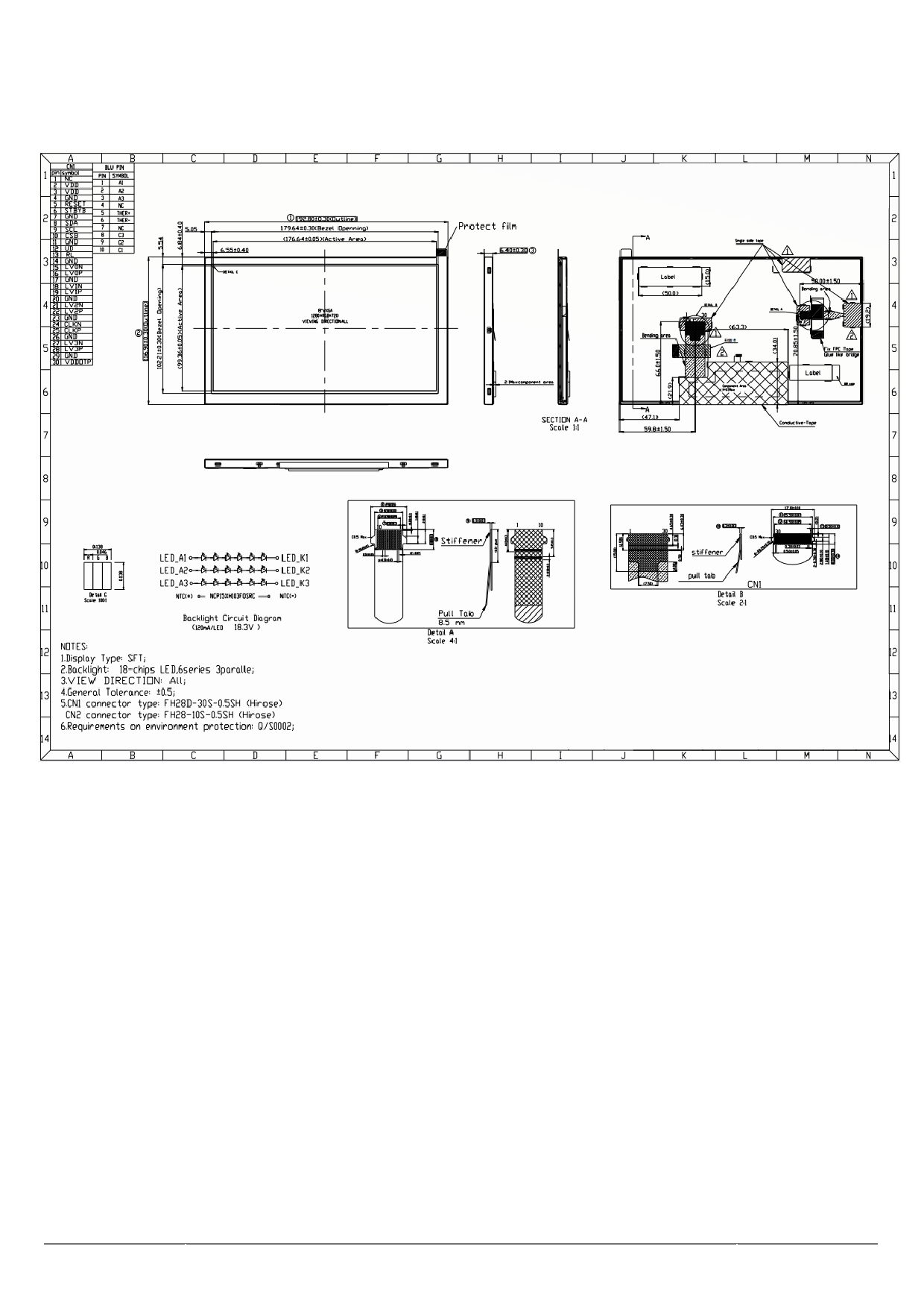
8. Mechanical Drawing
16