LMT121DNGFWD-NNC
LCD Module User Manual
Prepared by:
Checked by:
Approved by:
Lin Li
Date: 2019-06-24
Date:
Date:
Rev.
Descriptions
Release Date
0.1
Preliminary release
2019-06-24
URL: www.topwaydisplay.com
Document Name: LMT121DNGFWD-NNC-Manual-Rev0.1
Page: 1 of 13

TOPWAY
LCD Module User Manual
LMT121DNGFWD-NNC
Table of Content
1. General Specification ............................................................................................................ 3
2. Block Diagram ........................................................................................................................ 3
3. Terminal Function .................................................................................................................. 4
3.1
K1 TFT Input Terminal ........................................................................................................................................... 4
3.2
K2 Backlight Terminal ........................................................................................................................................... 4
3.3
K3 Capacitive Touch Panel Terminal ..................................................................................................................... 4
4. Absolute Maximum Ratings .................................................................................................. 5
5. Electrical Characteristics ...................................................................................................... 5
5.1
Driving TFT LCD Panel .......................................................................................................................................... 5
5.2
Driving For Backlight .............................................................................................................................................. 6
5.3
Capacitive Touch Panel ......................................................................................................................................... 6
5.4
Power supply voltage Sequence ............................................................................................................................ 7
6. AC Characteristics ................................................................................................................. 8
6.1
Input data mapping ................................................................................................................................................ 8
6.2
Timing Characteristics ............................................................................................................................................ 9
6.3
Input signal timing chart ......................................................................................................................................... 9
7. Physical Characteristics ..................................................................................................... 10
7.1
Optical Characteristics ......................................................................................................................................... 10
8. CTP Application Precautions .............................................................................................. 12
9. Precautions of Use of LCD Modules ................................................................................... 13
9.1
Handling Precautions ................................................................................................................. 错误 ! 未定义书签。
9.2
Storage precautions ................................................................................................................... 错误 ! 未定义书签。
9.3
Transportation Precautions ........................................................................................................ 错误 ! 未定义书签。
URL: www.topwaydisplay.com
Document Name: LMT121DNGFWD-NNC-Manual-Rev0.1
Page: 2 of 13
TOPWAY
LCD Module User Manual
LMT121DNGFWD-NNC
1. General Specification
TFT Interface :
LVDS (24bit or 18bit VESA )
CTP Interface:
Micro USB
Display Technology :
a-Si TFT active matrix
Display Mode :
Transmissive / Normal White
Screen Size(Diagonal) :
12.1”
Outline Dimension :
293.0x 232.0 x 15.9 (mm)
(see attached drawing for details)
Active Area :
245.76 x 184.32 (mm)
Number of dots :
1024 x 3 (RGB) x 768
Pixel Pitch :
0.240 x 0.240 (mm)
Pixel Configuration :
RGB Vertical Stripe
Backlight :
LED
Viewing Direction :
6 o’clock(Gray scale Inversion) (*1)
12 o’clock (*2)
Operating Temperature :
-20 ~ +70°C
Storage Temperature :
-30 ~ +80°C
Note:
*1. For saturated color display content (eg. pure-red, pure-green, pure-blue or pure-colors-combinations).
*2. For “color scales” display content.
*3. Color tone may slightly change by temperature and driving condition.
2. Block Diagram
D+,D-
5V
CTP Controller
Capacitive Touch Panel
GND
BLVCC,BLGND
BLADJ,BLEN
Backlight Circuit
1024(x3)x768 pixels
TFT Panel
VCC
GND
Source Driver
Source Driver
, RIN0-,RIN0+,RIN1-,RIN1+
RIN2-,RIN2+,RIN3-,RIN3+
LVDS interface
, CLK+,CLK-
, DPS,FRC
URL: www.topwaydisplay.com
Document Name: LMT121DNGFWD-NNC-Manual-Rev0.1
Page: 3 of 13
TOPWAY
LCD Module User Manual
LMT121DNGFWD-NNC
3. Terminal Function
3.1 K1 TFT Input Terminal (MSB240420HE)
Pin No. Pin Name
I/O
Descriptions
Input data signal: 8bit
Input data signal:6bit
1
VCC
2
VCC
Power
Power Supply(3.3V)
3
GND
Power
Ground(0V)
4
FRC
Input
High
Low or Open
5
RIN 0-
Input
LVDS receiver negative signal channel 0
6
RIN 0+
Input
LVDS receiver positive signal channel 0
7
GND
Power
Ground(0V)
8
RIN 1-
Input
LVDS receiver negative signal channel 1
9
RIN 1+
Input
LVDS receiver positive signal channel 1
10
GND
Power
Ground(0V)
11
RIN 2-
Input
LVDS receiver negative signal channel 2
12
RIN 2+
Input
LVDS receiver positive signal channel 2
13
GND
Power
Ground(0V)
14
CLKIN-
Input
LVDS receiver negative signal clock
15
CLKIN+
Input
LVDS receiver positive signal clock
16
GND
Power
Ground(0V)
17
RIN 3-
Input
LVDS receiver negative
signal channel 3
18
RIN 3+
Input
LVDS receiver positive signal Ground(0V)
channel 3
Selection of scan direction
19
DPS
Input
High: Reverse scan
Low or Open: Normal scan
20
NC
--
--
3.2 K2 Backlight Terminal(MSB24038P5)
Pin No Pin Name
I/O
Descriptions
1
NC
--
No connection
PWM Luminance control
2
BLADJ
Input
Hi:100%Drive
Lo:0% Drive
3
BLEN
Input
Backlight ON/OFF control:5V-On/0v-Off
4
BLGND
Power
Ground(0V)
5
BLVCC
Power
Backlight Power Supply(12V)
3.3 K3 Capacitive Touch Panel Terminal(Micro USB)
Pin No Pin Name
I/O
Descriptions
1
5V
Power
USB Power Supply(5V)
2
D-
I/O
USB D- signal
3
D+
I/O
USB D+ signal
4
GND
Power
Ground(0V)
5
GND
Power
Ground(0V)
URL: www.topwaydisplay.com
Document Name: LMT121DNGFWD-NNC-Manual-Rev0.1
Page: 4 of 13
TOPWAY
LCD Module User Manual
LMT121DNGFWD-NNC
4. Absolute Maximum Ratings
Items
Symbol Rating
Unit
Remarks
LCD panel signal processing
Power supply
VCC
-0.3 to +3.96
board
V
voltage
LED driver
BLVCC
-0.3 to (+15.0)
Display signals ,Note1
VD
-0.5 to 3.96
Ta= 25 ℃
V
Input voltage for
Function signals ,Note2
VF
-0.5 to 3.96
signals
BLADJ
-0.3 to (+15.0)
V
Function signal for LED driver
BLEN
-0.3 to (+15.0)
V
Storage temperature
Tst
-30 to +80
℃
-
Front surface
TopF
-20 to +70
℃
Note3
Operating temperature
Rear surface
TopR
-20 to +70
℃
Note4
Relative humidity
90
%
Ta ≤ 40 ℃
RH
Note5
85
%
40 ℃ < Ta ≤ 50 ℃
Absolute humidity ,Note5
AH
70,Note6
g/m3
Ta > 50 ℃
Note1:RIN0±,RIN1±,RIN2±,RIN3± and CLKIN±;
Note2:DPS and FRC;
Note3:Measured at LCD panel surface (including self-heat);
Note4:Measured at LCD module's rear shield surface (including self-heat);
Note5:No condensation;
Note6:Water amount at Ta= 50°C and RH= 85%.
5. Electrical Characteristics
5.1 Driving TFT LCD Panel
Ta=25 ℃
Items
Symbol
MIN.
TYP.
MAX.
Unit
Note
Power supply voltage
VCC
3.0
3.3
3.6
V
Power supply current
ICC
-
300
740
mA
*1
Permissible ripple voltage
VRP
-
-
300
mV
For VCC
Differential input threshold
VTL
-100
-
-
mV
VCM=1.25V,*2
voltage for LVDS receiver
VTH
-
-
100
mV
Terminating resistor
RT
-
100
-
Ω
Input voltage for DPS
VFH
0.7VCC
-
VCC
V
and FRC signals
VFL
0
-
0.3VCC
V
Note:
*1: All black pattern
*2: Common mode voltage for LVDS receiver
URL: www.topwaydisplay.com
Document Name: LMT121DNGFWD-NNC-Manual-Rev0.1
Page: 5 of 13
TOPWAY
LCD Module User Manual
LMT121DNGFWD-NNC
5.2 Driving For Backlight
BLGND=0V,Top=25 C
Parameter
Symbol
MIN.
TYP.
MAX.
Unit
Note
Power supply voltage
BLVCC
10.8
12.0
13.2
V
Note 1
Power supply voltage
I BLVCC
-
430
650
mA
At the maximum
Note2
luminance control
Permissible ripple voltage
VRPD
-
-
200
mVp-p
For BLVCC,Note3
Input voltage for PWM signal
VDFH1
2.0
-
BLVCC
V
VDFL1
0
-
0.8
V
Input voltage for BLEN signal
VDFH2
2.0
-
BLVCC
V
VDFL2
0
-
0.8
V
PWM Input Frequency
f PWM
200
-
20k
Hz
Note4,Note5
PWM duty ratio
DR PWM
1
-
100
%
Note6,Note7
PWM pulse width
tPWH
5
-
-
us
Note1:When designing of the power supply ,take the measures for the prevention of surge voltage.
Note2:This value excludes peak current such as overshoot current.
Note3:This power supply lines(BLVCC and GND)may have ripple voltage during luminance control of
LED.There is the possibility that the ripple voltage produces acoustic noise and signal wave
noise in audio circuit and so on.Put a capacitor between the power supply lines(BLVCC and
GND) to reduce the noise is necessary .
Note4:A recommended fPWM value is as follows.
f PWM = ( 2n-1 ) *fv/4
(n =integer,fv =frame frequency of LCD module )
Note5:Depending on the frequency used ,some noise may appear on the screen,please conduct a
thorough evaluation,
Note6:While the BLEN signal is high ,do not set the tPWH(PWM pulse width ) is less than 5us .It may
cause abnormal working is the backlight .In this case,turn the backlight off and then on again by
BLEN signal.
Note7:Regardless of the PWM frequency,both PWM duty radio and PWM pulse width must be always
more than the minimum values
5.3 Capacitive Touch Panel
T A =25 ℃
Items
Symbol MIN.
TYP.
MAX.
Unit
Note
Power supply voltage
5V
4.5
5.0
5.5
V
Power supply current
I 5V
-
TBD
-
mA
URL: www.topwaydisplay.com
Document Name: LMT121DNGFWD-NNC-Manual-Rev0.1
Page: 6 of 13
TOPWAY
LCD Module User Manual
LMT121DNGFWD-NNC
5.4
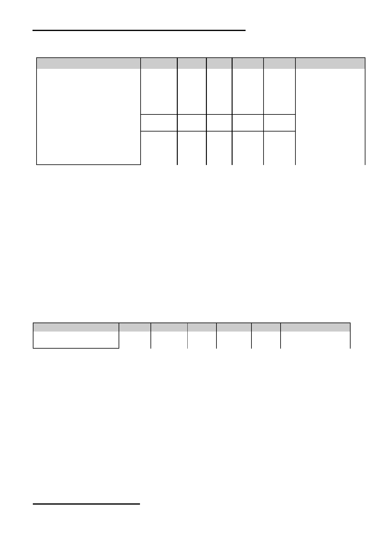
Power supply voltage Sequence
5.4.1 LCD panel signal processing board
Note1: If there is a voltage variation(voltage drop) at the rising edge of VCC below 3.0V,there is a
possibility that a product does not work due to a protection circuit.
Note2: Display signals (RIN0±,RIN1±,RIN2±,RIN3± and CLKIN±) and function signals(DPS and FRC) must
be set to Low or High-impedance, except the VALID period (See above sequence diagram),in
order to avoid the circuitry damage .If some of display and function signals of this product are cut
while this product is working, even if the signal input to it once again, it might not work normally. If a
customer stops the display and function signals, VCC also must be shut down.
5.4.2 LED Driver
Note1:These are the display and function signals for LCD panel signal processing board.
Note2:The backlight should be turned on within the valid period of display and function signals,in order to
avoid unstable data display.
URL: www.topwaydisplay.com
Document Name: LMT121DNGFWD-NNC-Manual-Rev0.1
Page: 7 of 13
TOPWAY
LCD Module User Manual
LMT121DNGFWD-NNC
6. AC Characteristics
6.1
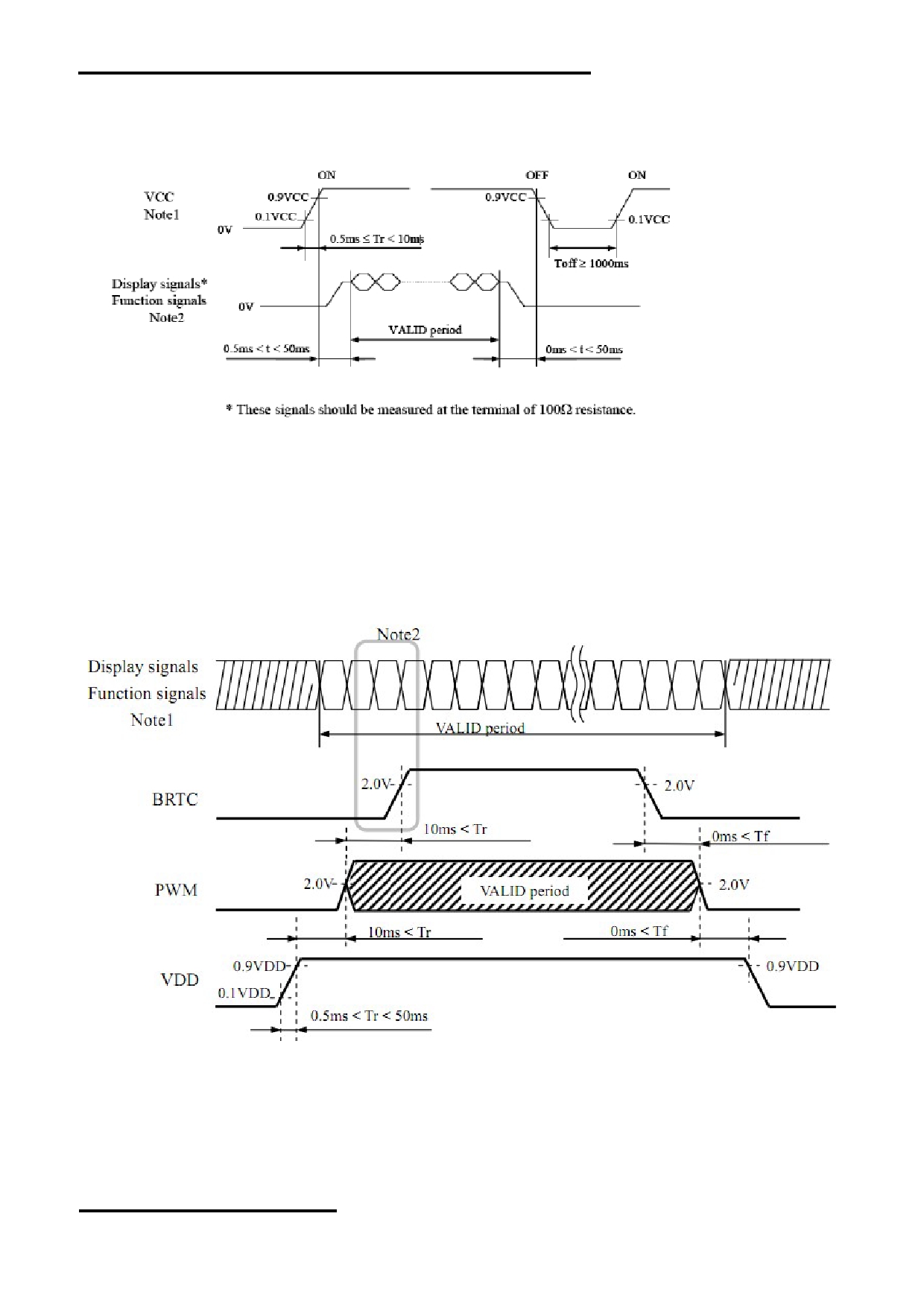
Input data mapping
(1) LVDS Input data signal: 8-bit
(2) LVDS Input data signal: 6-bit
URL: www.topwaydisplay.com
Document Name: LMT121DNGFWD-NNC-Manual-Rev0.1
Page: 8 of 13
TOPWAY
LCD Module User Manual
LMT121DNGFWD-NNC
6.2
Timing Characteristics
(Note1,Note2,Note3)
Parameter
Symbol MIN.
TYP.
MAX.
Unit
Remarks
Frequency
1/tc
52.0
65.0
71.0
MHz
15.385ns (typ.)
CLK
Duty ratio
-
-
-
-
Rise time, Fall time
-
ns
Setup time
-
ns
CLK-DATA
-
-
DATA
Hold time
-
ns
Rise time, Fall time
-
ns
-
16.542 20.676
26.88
us
Cycle
th
48.363kHz (typ.)
Horizontal
1114
1344
1400
CLK
Display period
thd
1024
CLK
-
DE
13.34 16.666
20.0
ms
Vertical
Cycle
tv
780
806
845
H
60.0Hz (typ.)
(One frame)
Display period
tvd
768
H
Setup time
-
ns
CLK-DE
-
-
Hold time
-
ns
Rise time, Fall time
-
ns
-
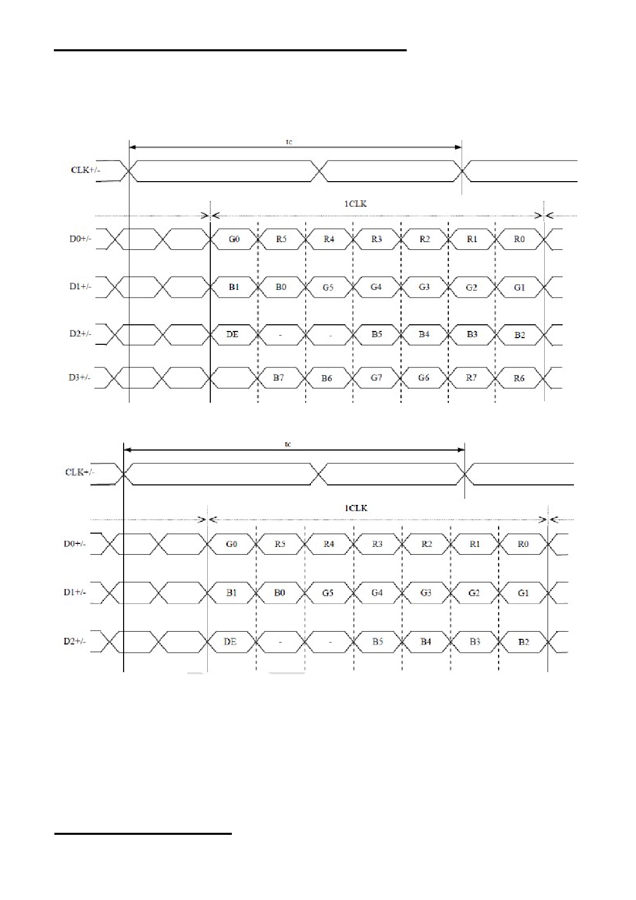
Note1:Definition of parameter is as follows.
tc = 1CLK , th = 1H
Note2:See the data sheet of LVDS transmitter.
ote3:Vertical cycle (tv) should be specified in integral multiple of Horizontal cycle (th).
6.3
Input signal timing chart
URL: www.topwaydisplay.com
Document Name: LMT121DNGFWD-NNC-Manual-Rev0.1
Page: 9 of 13
TOPWAY
LCD Module User Manual
LMT121DNGFWD-NNC
7. Physical Characteristics
7.1 Optical Characteristics
(Note*1,*2)
Measuring
Parameter
Condition
Symbol min.
typ.
max.
Unit
instrument
Remarks
White at center
Luminance
L
250
350
-
cd/m2 BM-5A
-
R= 0 , L= 0 , U= 0 , D= 0
White/Black at center
Contrast ratio
R= 0 , L= 0 , U= 0 , D= 0
CR
500
700
-
-
BM-5A
Note3
White
Luminance uniformity
R= 0 , L= 0 , U= 0 , D= 0
LU
-
1.25
(1.33)
-
BM-5A
Note6
x coordinate
Wx
0.263 0.313 0.363
-
White
y coordinate
Wy
0.279 0.329 0.379
-
x coordinate
Rx
-
TBD
-
-
Red
y coordinate
Ry
-
TBD
-
-
Chromaticity
x coordinate
Gx
-
TBD
-
-
Green
y coordinate
Gy
-
TBD
-
-
SR-3
Note5
x coordinate
Bx
-
TBD
-
-
Blue
y coordinate
By
-
TBD
-
-
Color gamut
R= 0 , L= 0 , U= 0 , D= 0
at center, against NTSC color space
C
48
55
-
%
White to Black
Ton
-
(3)
(5)
ms
Response time
BM-5A
Note4
Black to White
Toff
-
(5)
(8)
ms
-10000
Right
U= 0 , D= 0 , CR 10
R
70
80
-
Left
U= 0 , D= 0 , CR 10
L
70
80
-
Viewing angle
EZ
Up
R= 0 , L= 0 , CR 10
U
70
80
-
Note2
Contrast
Down
R= 0 , L= 0 , CR 10
D
70
80
-
Note:
*1. The value above are initial Characteristics.
* 2: Measurement conditions are as follows.
Ta= 25 ℃ , VCC= 3.3V, VDD= 12.0V, PWM duty ratio: 100%,
Display mode: XGA, Horizontal cycle= 1/48.363kHz, Vertical cycle= 1/60.0Hz,
DPS= Low or Open: Normal scan, FRC= High
URL: www.topwaydisplay.com
Document Name: LMT121DNGFWD-NNC-Manual-Rev0.1
Page: 10 of 13
TOPWAY
LCD Module User Manual
LMT121DNGFWD-NNC
Note 1:
Note 2:
The data are measured after LEDs are turned on for 5 minutes.
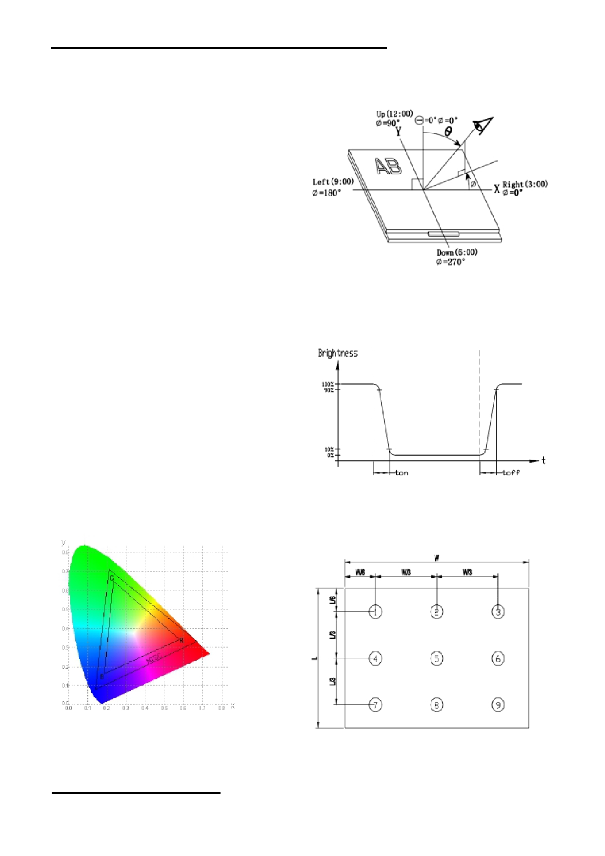
The definition of viewing angle:
LCM displays full white. The brightness is the average value of 9
Refer to the graph below marked by θ and Ф
measured spots. Measurement equipment SR-3A (1°)
Measuring condition:
- Measuring surroundings: Dark room
- Measuring temperature: Ta=25 ℃ .
- Adjust operating voltage to get optimum contrast at
the center of the display.
Note 4:
Note 3:
Definition of Response time. (Test LCD using BM-7A(2°)):
The definition of contrast ratio (Test LCM using SR-3A (1°)):
The output signals of photo detector are measured
Contrast
Luminance When LCD is at “White” state
when the input signals are changed from
Ratio(CR) = Luminance When LCD is at “Black” state
“black” to “white”(falling time)
(Contrast Ratio is measured in optimum common electrode
and from “white” to “black”(rising time), respectively.
voltage)
The response time is defined as
the time interval between the 10% and 90% of amplitudes.Refer to
figure as below.
Note 5:
Definition of Color of CIE1931 Coordinate and NTSC Ratio
Note 6:
Color gamut:
The luminance uniformity is calculated by using following formula
Bp = Bp (Min.) / Bp (Max.)×100 (%)
Area of RGB triangle
S =
X100%
Bp (Max.) = Maximum brightness in 9 measured spots
Area of NTSC triangle
Bp (Min.) = Minimum brightness in 9 measured spots .
Note 7:
Measured the luminance of white state at center point
URL: www.topwaydisplay.com
Document Name: LMT121DNGFWD-NNC-Manual-Rev0.1
Page: 11 of 13
TOPWAY
LCD Module User Manual
LMT121DNGFWD-NNC
8. CTP Application Precautions
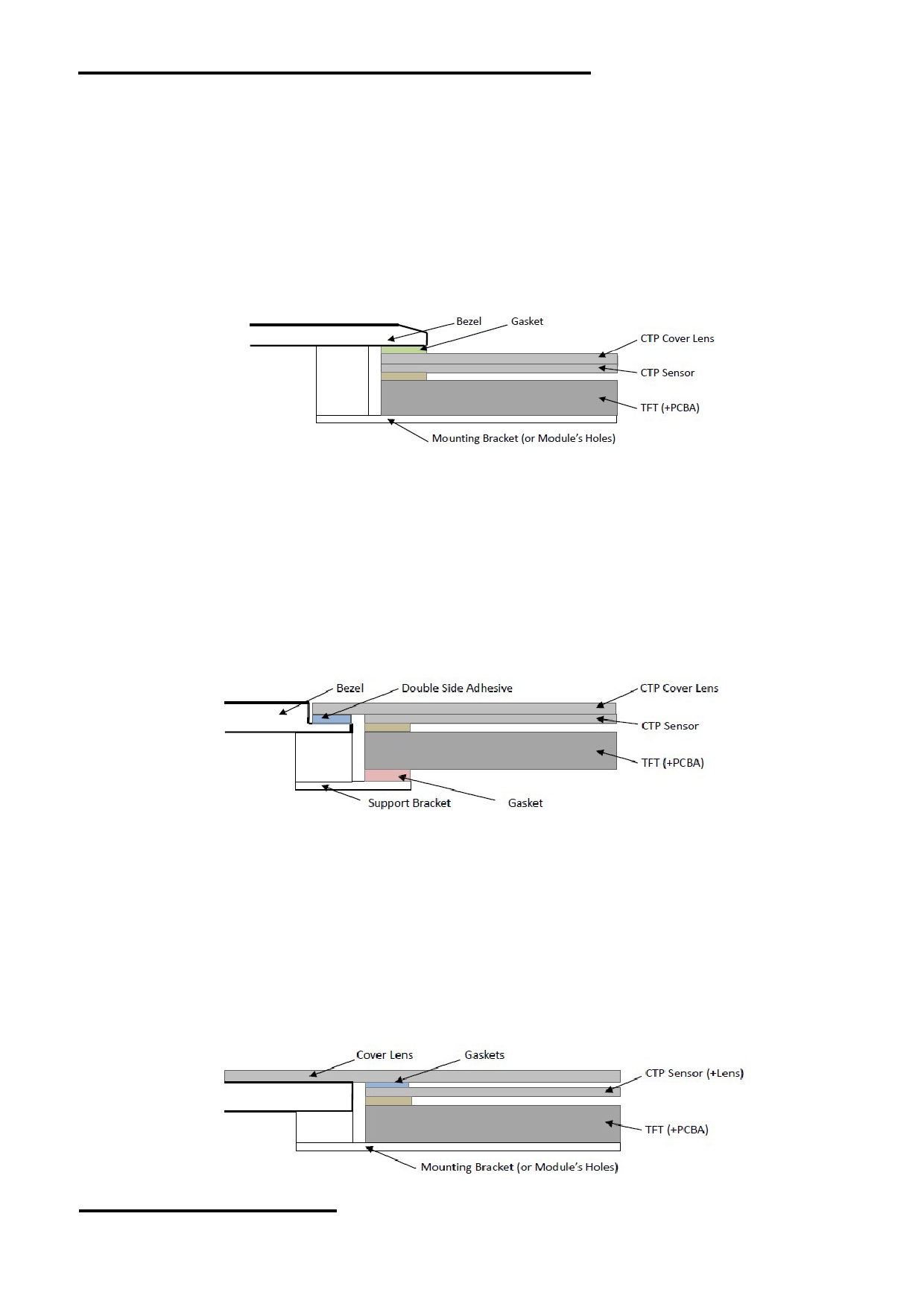
1. CTP Mounting Precaution
1.1 Bezel Mounting (Figure 1)
- The bezel window should be bigger than the CTP active area. It should be ≥ 0.5mm each side.
- Gasket
should be
installed
between
the bezel
and
the CTP
surface.
The final gap should be about 0.5~1.0mm.
- It is recommended to provide an additional support bracket for backside support when
necessary (e.g. slim type TFT module without mounding structure). They should only provide
appropriate support and keep the module in place.
- The mounting structure should be strong enough to prevent external uneven force or twist act
onto the module.
Figure 1
1.2 Surface Mounting (Figure 2)
- As the CTP assembling on the countersink area with double side adhesive.
The countersink area should be flat and clean to ensure the double side adhesive installation
result.
- The Bezel is recommend to keep a gap ( ≥ 0.3mm each side) around the cover lens for
tolerance.
- It is recommended to provide an additional support bracket with gasket for backside support
when necessary (e.g. TFT module without mounding structure). They should only provide
appropriate support and keep the module in place.
- The mounting structure should be strong enough to prevent external uneven force or twist act
onto the module.
Figure 2
1.3 Additional Cover Lens Mounting (Figure 3)
- For the case of additional cover Lens mounting, it is necessary to recheck with the CTP
specification about the material and thickness to ensure the functionality.
- It should keep a 0.2~0.3mm gap between the cover lens and the CTP surface..
- The cover lens window should be bigger than the active area of the CTP.
It should be ≥ 0.5mm each side.
- It is recommended to provide an additional support bracket for backside support when
necessary (e.g. slim type TFT module without mounding structure). They should only provide
appropriate support and keep the module in place.
- The mounting structure should be strong enough to prevent external uneven force or twist act
onto the module.
Figure 3
URL: www.topwaydisplay.com
Document Name: LMT121DNGFWD-NNC-Manual-Rev0.1
Page: 12 of 13

TOPWAY
LCD Module User Manual
LMT121DNGFWD-NNC
2. Handling Precautions
2.1 The product made of glass. Do not subject it to a mechanical shock by dropping it from a high
place, etc.
2.2 Do not apply excessive or uneven force to the product since this may damage to the
performance.
2.3 If the display surface is contaminated, breathe on the surface and gently wipe it with a soft dry
cloth. If still not completely clear, moisten cloth with Isopropyl alcohol or Ethyl alcohol solvents.
Solvents other than those mentioned above may damage the product. Especially, do not use
Water, Ketone, Aromatic solvents.
2.4 Do not attempt to disassemble the CTP Module.
2.5 If the logic circuit power is off, do not apply the input signals.
2.6 To prevent destruction of the elements by static electricity, be careful to maintain an optimum
work environment.
a. Be sure to ground the body when handling the CTP Modules.
b. Tools required for assembly, such as soldering irons, must be properly ground.
c. To reduce the amount of static electricity generated, do not conduct assembly and other work
under dry conditions.
d. The CTP Module is coated with a film to protect the display surface. Be care when peeling off
this protective film since static electricity may be generated.
3. Storage and Transportation Precautions
3.1 When storing the CTP modules, avoid exposure to direct sunlight or to the light of fluorescent
lamps.
3.2 The CTP modules should be stored the required temperature range. If the CTP modules will be
stored for a long time, the recommend condition is the temperature of 0~40 ℃ and relative
humidity of ≤ 80%.
3.3 The LCD modules should be stored in the room without acid, alkali and harmful gas.
3.4 The CTP modules should be no falling and violent shocking during transportation, and also
should avoid excessive press, water, damp and sunshine.
9. Precautions of Use of LCD Modules
Please refer to "LCD-Module-Design-Handling-Precaution.pdf".
URL: www.topwaydisplay.com
Document Name: LMT121DNGFWD-NNC-Manual-Rev0.1
Page: 13 of 13