LMT150FNGFSA
LCD Module User Manual
Prepared by:
Checked by:
Approved by:
LuoLin
Date: 2026-09-28
Date:
Date:
Rev. Descriptions
Edit
Release Date
0.1
Preliminary release
LuoLin
2026-09-28
URL: www.topwaydisplay.com
Document Name: LMT150FNGFSA-Manual-Rev0.1.DOC
Page 1 of 30

TOPWAY
LCD Module User Manual
LMT150FNGFSA
-
CONTENTS
1.
Summary ....................................................................................................................................... 4
1.1
General Description ............................................................................................................. 4
1.2
Features .............................................................................................................................. 4
2. General Specifications ................................................................................................................... 5
3.
Input /Output Terminals ................................................................................................................ 6
4.
Absolute Maximum Ratings .......................................................................................................... 10
5.
Electrical Characteristics .............................................................................................................. 11
6. Timing Chart ................................................................................................................................ 15
7.
Optical Characteristics ................................................................................................................. 24
8.
Environmental / Reliability Test .................................................................................................... 27
9.
Mechanical drawing ..................................................................................................................... 28
10.
Precautions for Use of LCD Modules ......................................................................................... 30
URL: www.topwaydisplay.com
Document Name: LMT150FNGFSA-Manual-Rev0.1.DOC
Page 2 of 30

TOPWAY
LCD Module User Manual
LMT150FNGFSA
-
1.
Summary
1.1
General Description
This is a 15 inch a-Si TFT-LCD module with Normal- black technology. It is composed of a TFT-LCD
panel, a driver circuit, PCBA, BEZEL, and a LED backlight unit.
1.2
Features
Amending Annex II of 2011/65/EU)
URL: www.topwaydisplay.com
Document Name: LMT150FNGFSA-Manual-Rev0.1.DOC
Page 4 of 30
TOPWAY
LCD Module User Manual
LMT150FNGFSA
-
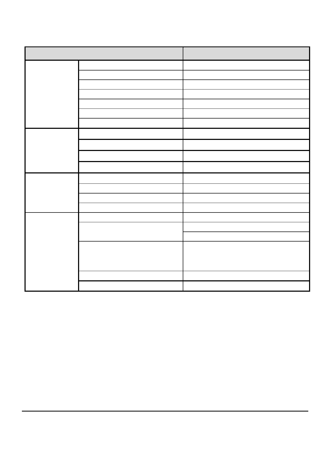
2.
General Specifications
Feature
Spec
Size (inch)
15
Resolution
1024*768
Technology Type
SFT
Display Spec.
Pixel Configuration
B.G.R vertical stripe
Pixel Pitch (mm)
0.297 x 0.297
Display Mode
Transmissive, Normally Black
Surface Treatment (Up Polarizer)
Antiglare
Luminance (cd/m2)
1700 Typ.
Optical
Contrast ratio
1000:1 Typ.
Characteristics
Response time Ton+Toff (ms)
25 Typ.
Viewing angle R/L/U/D (Degree)
89/89/89/89 Typ
LCM (W x H x D) (mm)
326.5 x 253.5 x 13 Typ.
Mechanical
Active Area (mm)
304.128 x 228.096
Characteristics
With /Without TSP
Without TSP
Weight (g)
1048g
Interface
1port LVDS
LCD panel: 3.3 Typ.
Power supply voltage (V)
Backlight: 12V Typ.
Electrical
16,194,277 colors
(At 8-bit input, FRC terminal= Low)
Characteristics
Color Depth
262,144 colors
(At 6-bit input, FRC terminal=High or Open)
Backlight LED driver
Build in LCM
Power consumption (W)
LCD+Backlight : 34.02W
Note 1 : Requirements on Environmental Protection: Q/S0002+UL
Note 2 : LCM weight max. tolerance : +10%
URL: www.topwaydisplay.com
Document Name: LMT150FNGFSA-Manual-Rev0.1.DOC
Page 5 of 30
TOPWAY
LCD Module User Manual
LMT150FNGFSA
-
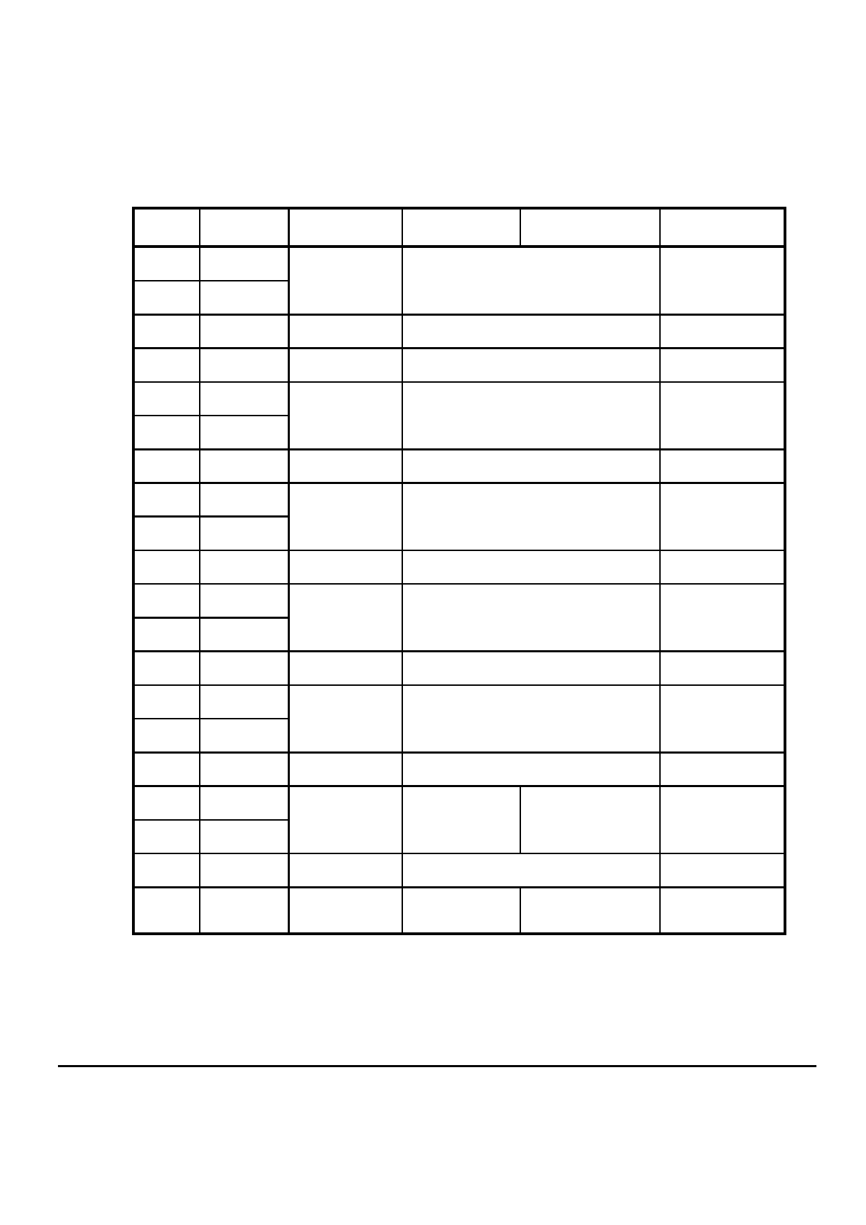
3.1
TFT LCD Panel
CN1 socket (LCD module side):
MSB240420HE ( STM )
Adaptable plug: P240420H
Pin No.
Symbol
Signal
Input data signal:
Input data signal:
8-bit
6-bit
Remarks
1
VCC
Power supply
Power supply
Note2
2
VCC
3
GND
Ground
Ground
Note2
4
DPS
Selection
High :
Reverse scan
of scan direction
Low or Open :
Normal scan
Note3
5
D0-
Pixel data
R0-R5, G0
Note1
6
D0+
7
GND
Ground
Ground
Note2
8
D1-
Pixel data
G1-G5, B0-B1
Note1
9
D1+
10
GND
Ground
Ground
Note2
11
D2-
Pixel data
B2-B5, DE
Note1
12
D2+
13
GND
Ground
Ground
Note2
14
CLK-
Pixel clock
Pixel clock
Note1
15
CLK+
16
GND
Ground
Ground
Note2
17
D3-/ GND
Pixel data
R6-R7
/ Ground
G6-G7
Ground
Note1
18
D3+/ GND
B6-B7
19
N.C.
Non connection
-
Keep this pin Open
Selection of the
20
FRC
number of
Low or Open
High
Note4,
colors
Note5
Note1: All GND and VCC terminals should be used without any non-connected lines.
Note2: Twist pair wires with 100 (Characteristic impedance) should be used between LCD
panel signal processing board and LVDS transmitter.
Note3: See " 6.6 SCANNING DIRECTIONS ".
Note4: See " 6.4 DISPLAY COLORS AND INPUT DATA SIGNALS ".
Note5: See " 2.4 Connection between receiver and transmitter for LVDS ".
URL: www.topwaydisplay.com
Document Name: LMT150FNGFSA-Manual-Rev0.1.DOC
Page 6 of 30
TOPWAY
LCD Module User Manual
LMT150FNGFSA
-
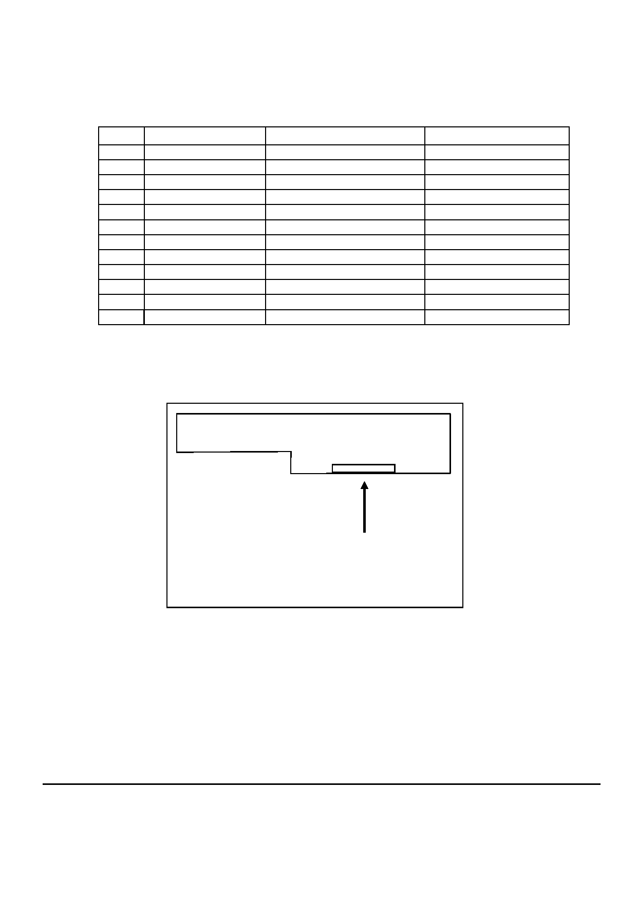
3.2 Backlight
CN2 socket (LCD module side):
5040501291(Molex)
Adaptable plug: 5040511201
Pin No.
Symbol
Signal
Remarks
1
VDD
Backlight power input
2
VDD
Backlight power input
3
VDD
Backlight power input
4
VDD
Backlight power input
5
GND
Backlight power GND
6
GND
Backlight power GND
7
GND
Backlight power GND
8
GND
Backlight power GND
9
NC
Non connection
10
NC
Non connection
11
BRTC
Backlight ON/OFF EN
12
PWM
Backlight PWM
Note1: All GND and VDD terminals should be used without any non-connected lines.
3.3 Positions of Socket
Rear side
CN
1
20
1
Insert
direction
URL: www.topwaydisplay.com
Document Name: LMT150FNGFSA-Manual-Rev0.1.DOC
Page 7 of 30
TOPWAY
LCD Module User Manual
LMT150FNGFSA
-
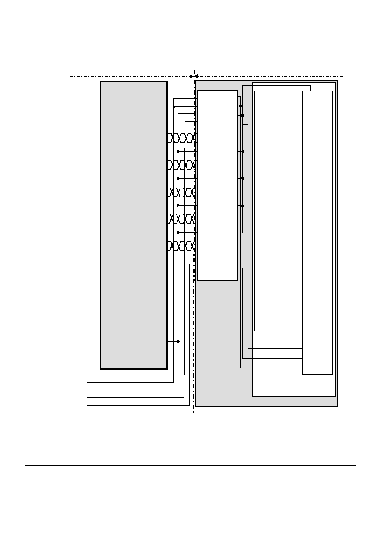
3.4 Connection between receiver and transmitter for LVDS
(1) LVDS Input data signal: 8-bit (FRC: Low or Open )
Host
LCD module (Product)
Note2
R0
TA0
Note3
R1
TA1
1
VCC
GND
R2
TA2
2
VCC
R3
TA3
3
GND
R4
TA4
4
DPS
R5
TA5
TA-
5
D0-
RA-
G0
TA6
TA+
6
D0+
RA+
7
GND
G1
TB0
TB-
8
D1-
RB-
G2
TB1
TB+
9
D1+
RB+
G3
TB2
10
GND
G4
TB3
TC-
11
D2-
RC-
G5
TB4
TC+
12
D2+
RC+
Signal
B0
TB5
13
GND
processo
B1
TB6
TCLK-
14
CLK-
RCLK-
r
TCLK+
15
CLK+
RCLK+
B2
TC0
16
GND
B3
TC1
TD-
17
D3-
RD-
B4
TC2
TD+
18
D3+
RD+
B5
TC3
19
N. C.
Note4
TC4
20
FRC
Note4
TC5
Receiver for LVDS
DE
TC6
CN1
R6
TD0
R7
TD1
G6
TD2
G7
TD3
B6
TD4
GND
B7
TD5
Note4
TD6
DPS
CLK
CLK IN
FRC
LVDS transmitter
Note1
THC63LVDM83C(5S) or equivalent
VCC
VCC
GND
LCD controller
DPS
LCD panel signal processing board
FRC
Note1: Recommended transmitter: THC63LVDM83C (5S) (THine Electronics Inc.) or equivalent.
Note2: LSB (Least Significant Bit) - R0, G0, B0. MSB (Most Significant Bit) - R7, G7, B7
Note3: Twist pair wires with 100 (Characteristic impedance) should be used between
LCD panel signal processing board and LVDS transmitter.
Note4: Input signals to TC4, TC5 and TD6 are not used inside the product, but do not keep
them open to avoid noise problem.
URL: www.topwaydisplay.com
Document Name: LMT150FNGFSA-Manual-Rev0.1.DOC
Page 8 of 30
TOPWAY
LCD Module User Manual
LMT150FNGFSA
-
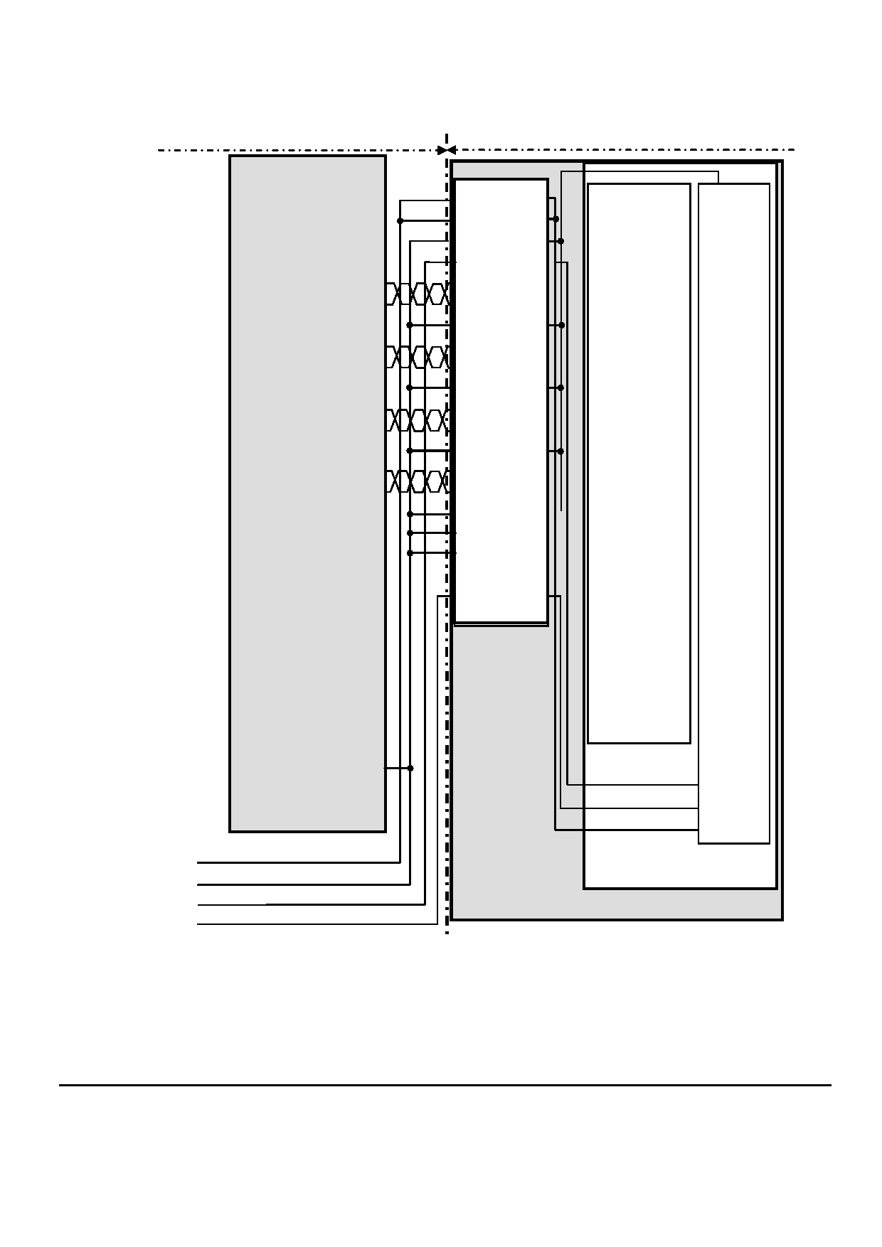
(2) LVDS Input data signal: 6-bit (FRC: High)
Host
LCD module (Product)
Note2
R0
TA0
Note3
R1
TA1
1
VCC
GND
R2
TA2
2
VCC
R3
TA3
3
GND
R4
TA4
4
DPS
R5
TA5
TA-
5
D0-
RA-
G0
TA6
TA+
6
D0+
RA+
7
GND
G1
TB0
TB-
8
D1-
RB-
G2
TB1
TB+
9
D1+
RB+
G3
TB2
10
GND
G4
TB3
TC-
11
D2-
RC-
G5
TB4
TC+
12
D2+
RC+
Signal
B0
TB5
13
GND
processor
B1
TB6
TCLK-
14
CLK-
RCLK-
TCLK+
15
CLK+
RCLK+
B2
TC0
16
GND
B3
TC1
TD-
17
GND
B4
TC2
TD+
18
GND
B5
TC3
19
N. C.
Note4
TC4
20
FRC
Note4
TC5
Receiver for LVDS
DE
TC6
Note4
TD0
Note4
TD1
Note4
TD2
Note4
TD3
Note4
TD4
GND
Note4
TD5
DPS
Note4
TD6
FRC
CLK
CLK IN
VCC
LVDS transmitter
Note1
THC63LVDM83C (5S) or equivalent
VCC
LCD controller
GND
DPS
LCD panel signal processing board
FRC
Note1: Recommended transmitter: THC63LVDM83C (5S) (THine Electronics Inc.) or equivalent.
Note2: LSB (Least Significant Bit) - R0, G0, B0. MSB (Most Significant Bit) - R5, G5, B5
Note3: Twist pair wires with 100 (Characteristic impedance) should be used between
LCD panel signal processing board and LVDS transmitter.
Note4: Input signals to TC4, TC5 and TD0-6 are not used inside the product, but do not
keep them open to avoid noise problem.
URL: www.topwaydisplay.com
Document Name: LMT150FNGFSA-Manual-Rev0.1.DOC
Page 9 of 30
TOPWAY
LCD Module User Manual
LMT150FNGFSA
-
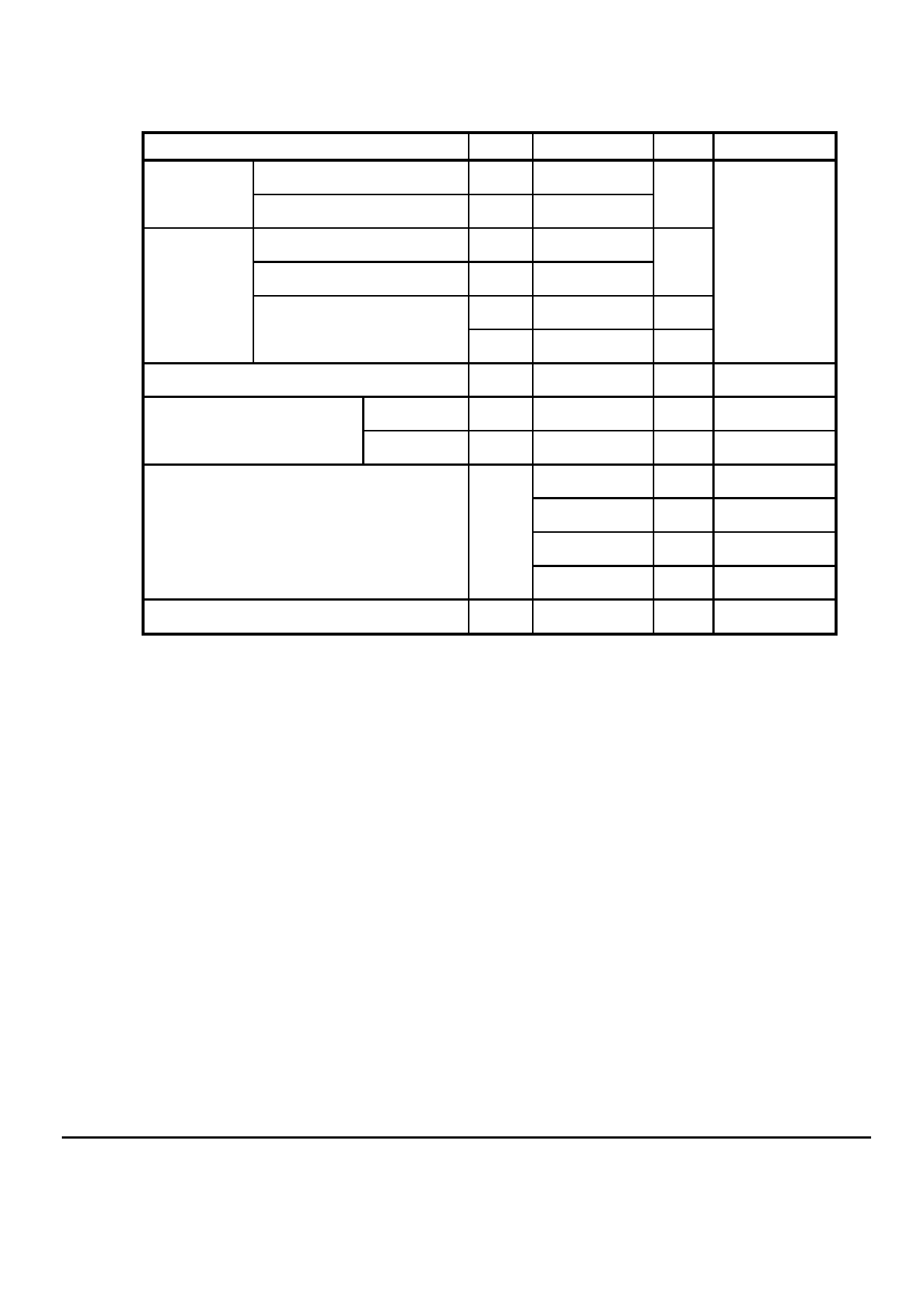
4.
Absolute Maximum Ratings
Parameter
Symbol
Rating
Unit
Remarks
LCD panel signal processing
VCC
-0.3 to +3.96
Power supply
board
voltage
V
LED driver
VDD
-0.3 to +15.0
Display signals
Note1
VD
-0.5 to VCC+0.3
V
Ta= 25 C
Function signals
VF
-0.5 to VCC+0.3
Input voltage
Note2
for signals
PWM
-0.3 to +5.5
V
Function signal for LED driver
BRTC
-0.3 to +5.5
V
Storage temperature
Tst
-40 to +85
C
-
Front surface
TopF
-30 to +70
C
Note3
Operating temperature
Rear surface
TopR
-30 to +70
C
Note4
95
%
Ta 40 C
%
Relative humidity
85
40 C < Ta 50 C
Note5
RH
55
%
50 C < Ta 60 C
36
%
60 C < Ta 70 C
Absolute humidity
70
g/m
3
Note5
AH
Note6
Ta > 70 C
Note1: D0+/-, D1+/-, D2+/-, D3+/- and CLK+/-
Note2: DPS and FRC
Note3: Measured at LCD panel surface (including self-heat)
Note4: Measured at LCD module's rear shield surface (including self-heat)
Note5: No condensation
Note6: Water amount at Ta= 70°C and RH= 36%
URL: www.topwaydisplay.com
Document Name: LMT150FNGFSA-Manual-Rev0.1.DOC
Page 10 of 30
TOPWAY
LCD Module User Manual
LMT150FNGFSA
-
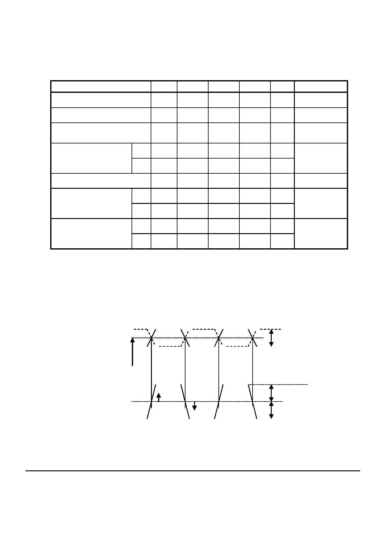
5.
Electrical Characteristics
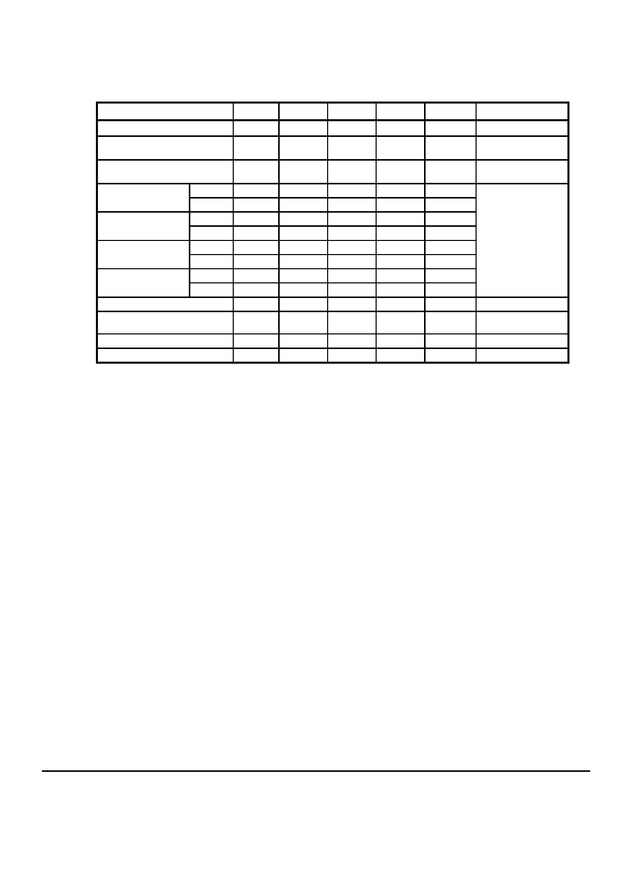
5.1 Driving TFT LCD Panel
(Ta= 25 C)
Parameter
Symbol
min.
typ.
max.
Unit
Remarks
Power supply voltage
VCC
3.0
3.3
3.6
V
-
Power supply current
ICC
-
290
-
mA
at VCC= 3.3V
for VCC
Permissible ripple voltage
VRP
-
-
200
mVp-p
Note3
Note4,Note5
High
VTH
-
-
+100
mV
Differential input threshold
at VCM= 1.25V
voltage
Note6 , 7
Low
VTL
-100
-
-
mV
Terminating resistance
RT
-
100
-
-
High
VFH
0.7VCC
-
VCC
V
Input voltage for DPS and
FRC signals
-
Low
VFL
0
-
0.3VCC
V
High
IFH
-
-
500
A
Input current for DPS and
FRC signals
-
Low
IFL
-500
-
-
A
Note1: Checkered flag pattern [by IEC 61747-6]
Note2: Pattern for maximum current
Note3: This product works even if the ripple voltage levels are over the permissible values,
but there might be noise on the display image.
Note4: The permissible ripple voltage includes spike noise.
Note5: The load variation influence does not include.
Note6: Common mode voltage for LVDS receiver
Note7: DC characteristics (LVDS receiver part)
C L K _ P , D x _ P
| V I D |
C L K _ N , D x _ N
V C M
D i f f e r e n t i a l
C L K , D x
| V I D |
V T H
D i f f e r e n t i a l = 0 V
V T L
| V I D |
URL: www.topwaydisplay.com
Document Name: LMT150FNGFSA-Manual-Rev0.1.DOC
Page 11 of 30
TOPWAY
LCD Module User Manual
LMT150FNGFSA
-
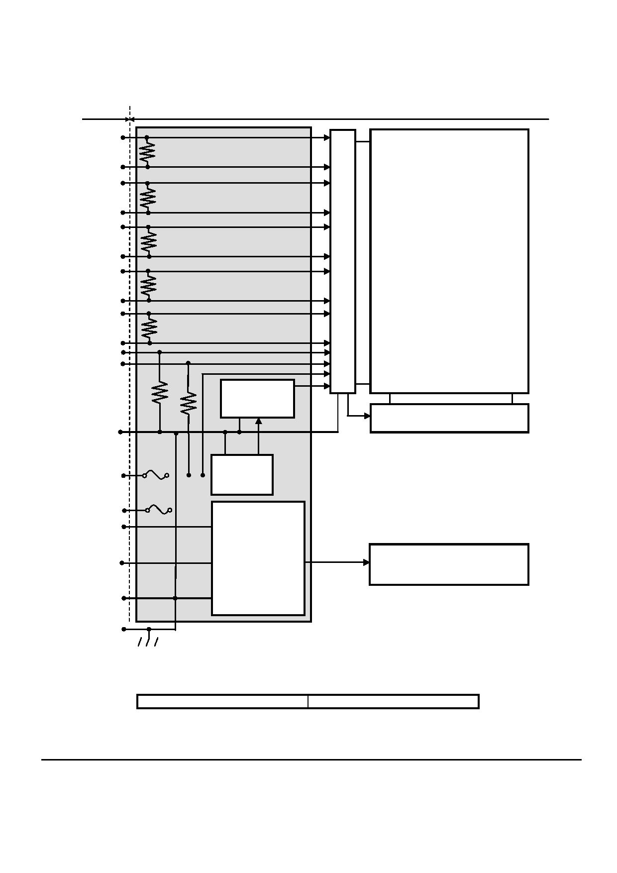
5.2 Driving Backlight
(Ta= 25 C)
Parameter
Symbol
min.
typ.
max.
Unit
Remarks
Power supply voltage
VDD
10.8
12
13.2
V
Note1
Power supply current
IDD
-
2755
-
mA
At the maximum
luminance control
Permissible ripple voltage
VRPD
-
-
500
mVp-p
for VDD
Note3,Note4,Note5
Input voltage for
High
VDFH1
1.8
-
5.3
V
PWM signal
Low
VDFL1
0
-
0.8
V
Input voltage for
High
VDFH2
1.8
-
5.3
V
BRTC signal
Low
VDFL2
0
-
0.8
V
Note6
Input current for
High
IDFH1
-
-
800
A
PWM signal
Low
IDFL1
-800
-
-
A
Input current for
High
IDFH2
-
-
800
A
BRTC signal
Low
IDFL2
-800
-
-
A
PWM frequency
f PWM
200
-
10k
Hz
Note7, Note9
PWM duty ratio
DR PWM
1
-
100
%
Note8,
Note10,Note11
PWM pulse width
tPWH
5
-
-
s
Note10,Note11
LED life time
Hr
50000
Hour
Note 11
Note1: When designing of the power supply, take the measures for the prevention of surge
voltage.
Note2: This value excludes peak current such as overshoot current.
Note3: The power supply lines (VDD and GND) may have ripple voltage during luminance
control of LED. There is the possibility that the ripple voltage produces acoustic
noise and signal wave noise in audio circuit and so on.
Note4: The permissible ripple voltage includes spike noise.
Note5: This product works if the ripple voltage levels are over the permissible values, but
there might be noise on the display image.
Note6: See " 5.3 BLOCK DIAGRAM ".
Note7: A recommended f PWM value is as follows.
2n 1
f
PWM
fv
4
(n integer, fv frame frequency of LCD module)
Note8:
DR
PWM
=
tPWH
tPW
tPWH: PWM pulse width, tPW: PWM dimming cycle (= 1/f PWM )
Note9: Depending on the frequency used, some noise may appear on the screen, please
conduct a thorough evaluation.
Note10: While the BRTC signal is high, do not set the tPWH (PWM pulse width) is less than
minimum value. It may cause abnormal working of the backlight. In this case, turn
the backlight off and then on again by BRTC signal.
Note11: Regardless of the PWM frequency, both PWM duty ratio and PWM pulse width
must be always more than the minimum values.
Note12: Optical performance should be evaluated at Ta=25 ℃ .Only If LED is driven by high
current, high ambient temperature & humidity condition. The life time of LED will be
reduced. Operating life means brightness goes down to 50% of initial brightness.
Typical operating life time is an estimated data.
URL: www.topwaydisplay.com
Document Name: LMT150FNGFSA-Manual-Rev0.1.DOC
Page 12 of 30
TOPWAY
LCD Module User Manual
LMT150FNGFSA
-
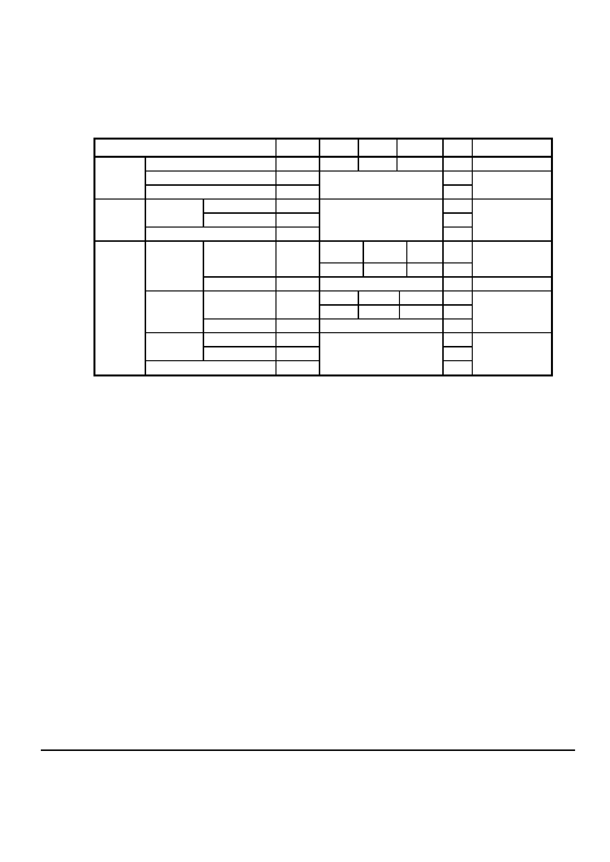
5.3 Block Diagram
Host
LCD module (Product)
D0+
100
D0-
LCD panel
D1+
100
D1-
H: 1024 × 3 (B, G, R)
V: 768
D2+
100
D2-
D3+
100
D3-
CLK+
100
CLK-
DPS
FRC
768 lines
Power supply
for gradation
V-driver
GND
Note1
Note2
Fuse
DC/DC
VCC
converter
Fuse
VDD
PWM
BRTC
LED driver
LED Backlight
GND
FG
LCD panel signal processing board
Note1: Relations between GND (Signal ground) and FG (Frame ground) in the LCD
module are as follows.
GND - FG
Connected
Note2: GND and FG must be connected to customer equipment ’ s ground, and it is
recommended that these grounds be connected together in customer equipment.
URL: www.topwaydisplay.com
Document Name: LMT150FNGFSA-Manual-Rev0.1.DOC
Page 13 of 30

TOPWAY
LCD Module User Manual
LMT150FNGFSA
-
5.4 Fuse
Fuse
Parameter
Rating
Fusing current
Remarks
Type
Supplier
1.5A
VCC
FCC16152AB
KAMAYA ELECTRIC
Co., Ltd.
3.0A
36V
KAMAYA ELECTRIC
5.0A
Note1
VDD
SMFD1206P50
0
Co., Ltd.
10.0A
PTTC
63V
Note1: The power supply ’ s rated current must be more than the fusing current. If it is less
than the fusing current, the fuse may not blow in a short time, and then nasty smell,
smoke and so on may occur.
URL: www.topwaydisplay.com
Document Name: LMT150FNGFSA-Manual-Rev0.1.DOC
Page 14 of 30
TOPWAY
LCD Module User Manual
LMT150FNGFSA
-
6.
Timing Chart
6.1
Timing Characteristics
(Note1, Note2, Note3)
Parameter
Symbol
min.
typ.
max.
Unit
Remarks
Frequency
1/tc
58.4
65.0
67.9
MHz
15.385 ns (typ.)
CLK
Duty ratio
-
-
-
-
Rise time, Fall time
-
ns
Setup time
-
ns
CLK-DATA
DATA
Hold time
-
-
ns
-
Rise time, Fall time
-
ns
20.202
20.676
21.01
s
Cycle
th
7
48.363 kHz
Horizontal
(typ.)
1229
1,344
1372
CLK
Display period
thd
1024
CLK
-
Vertical
-
16.666
-
ms
DE
Cycle
tv
(One
793
806
825
H
60.0 Hz (typ.)
frame)
Display period
tvd
768
H
Setup time
-
ns
CLK-DE
Hold time
-
-
ns
-
Rise time, Fall time
-
ns
Note1: Definition of parameters is as follows.
tc= 1CLK, th= 1H
Note2: See the data sheet of LVDS transmitter.
Note3: Vertical cycle (tv) should be specified in integral multiple of Horizontal cycle (th).
URL: www.topwaydisplay.com
Document Name: LMT150FNGFSA-Manual-Rev0.1.DOC
Page 15 of 30
TOPWAY
LCD Module User Manual
LMT150FNGFSA
-
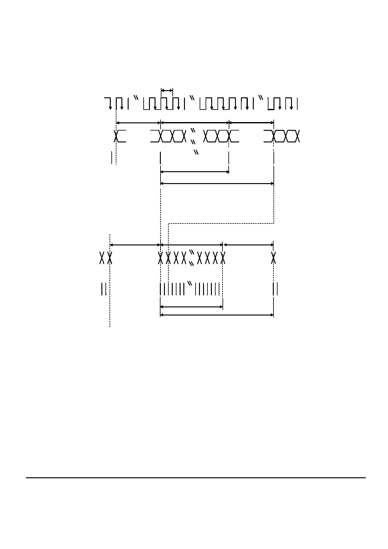
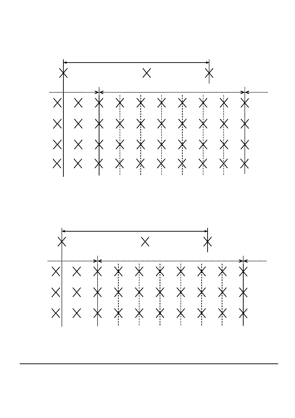
6.2 Input Signal Timing Chart
Horizontal timing
tc
CLK
INVALID
VALID
INVALID
DATA
Note1
1
2
1023 1024
DE
thd (1024CLK)
th (1344CLK)
Vertical timing
INVALID
VALID
INVALID
DATA
Note1
1 2
767 768
DE
tvd (768H)
tv (806H)
Note1:
DATA = R0-R7, G0-G7, B0-B7 or R0-R5, G0-G5, B0-B5.
URL: www.topwaydisplay.com
Document Name: LMT150FNGFSA-Manual-Rev0.1.DOC
Page 16 of 30
TOPWAY
LCD Module User Manual
LMT150FNGFSA
-
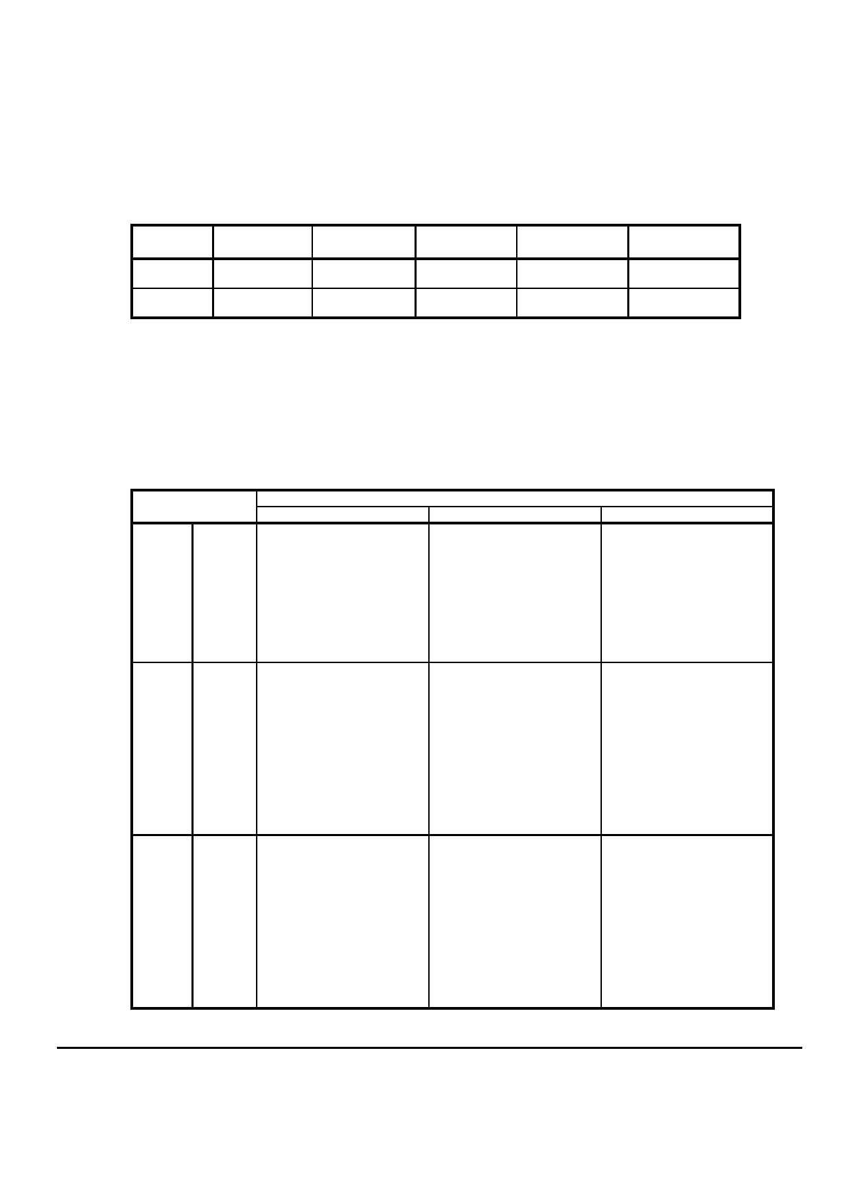
6.3 Input Data Mapping
(1) Input data signal: 8-bit
tc
CLK+/-
1CLK
D0+/-
G0
R5
R4
R3
R2
R1
R0
D1+/-
B1
B0
G5
G4
G3
G2
G1
D2+/-
DE
-
B5
B4
B3
B2
-
D3+/-
--
B7
B6
G7
G6
R7
R6
-
Note1: LSB (Least Significant Bit) - R0, G0, B0. MSB (Most Significant Bit) – R7, G7, B7
Note2: Twist pair wires with 100 (Characteristic impedance) should be used between LCD
panel signal processing board and LVDS transmitter.
(2) Input data signal: 6-bit
tc
CLK+/-
1CLK
D0+/-
G0
R5
R4
R3
R2
R1
R0
D1+/-
B1
B0
G5
G4
G3
G2
G1
D2+/-
DE
-
-
B5
B4
B3
B2
Note1: LSB (Least Significant Bit) - R0, G0, B0. MSB (Most Significant Bit) – R5, G5, B5
Note2: Twist pair wires with 100 (Characteristic impedance) should be used between LCD
panel signal processing board and LVDS transmitter.
URL: www.topwaydisplay.com
Document Name: LMT150FNGFSA-Manual-Rev0.1.DOC
Page 17 of 30
TOPWAY
LCD Module User Manual
LMT150FNGFSA
-
6.4 Display Colors and Input Data Signals
6.4.1 Combinations of input data signals and FRC signal
This product can display 16,194,277 colors with 253 gray scales and 262,144 colors with 64
gray scales by combination of input data signals and FRC signal. See the following table.
Combinatio
Input data
CN1-
n
signals
Pin No.17 and 18
FRC terminal
Display colors
Remarks
①
8-bit
D3+/-
Low
16,194,277
Note1
②
6-bit
GND
High or Open
262,144
Note2
Note1: See " 6.4.2 16,194,277 colors ".
Note2: See " 6.4.3 262,144 colors ".
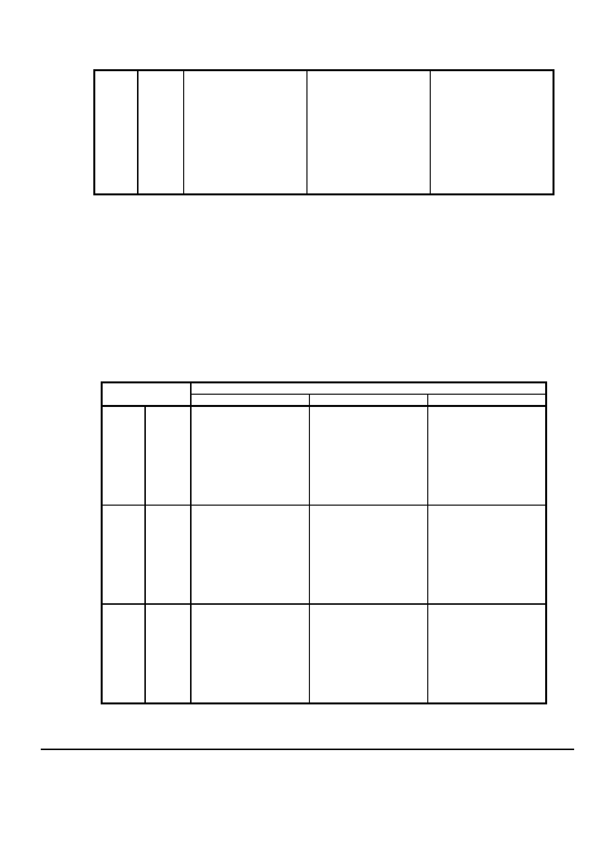
6.4.2 16,194,277 colors
This product can display 16,194,277 colors with 253 gray scales by combination ① .
(See " 6.4.1 Combinations of input data signals and FRC signal ".)
Also the relation between display colors and input data signals is as follows.
Data signal (0: Low level, 1: High level)
Display colors
R7 R6 R5 R4 R3 R2 R1 R0
G7 G6 G5 G4 G3 G2 G1 G0
B7 B6 B5 B4 B3 B2 B1 B0
Black
0
0
0
0
0
0
0
0
0
0
0
0
0
0
0
0
0
0
0
0
0
0
0
0
Blue
0
0
0
0
0
0
0
0
0
0
0
0
0
0
0
0
1
1
1
1
1
1
0
0
Red
1
1
1
1
1
1
0
0
0
0
0
0
0
0
0
0
0
0
0
0
0
0
0
0
Magenta
1
1
1
1
1
1
0
0
0
0
0
0
0
0
0
0
1
1
1
1
1
1
0
0
Green
0
0
0
0
0
0
0
0
1
1
1
1
1
1
0
0
0
0
0
0
0
0
0
0
Cyan
0
0
0
0
0
0
0
0
1
1
1
1
1
1
0
0
1
1
1
1
1
1
0
0
Yellow
1
1
1
1
1
1
0
0
1
1
1
1
1
1
0
0
0
0
0
0
0
0
0
0
White
1
1
1
1
1
1
0
0
1
1
1
1
1
1
0
0
1
1
1
1
1
1
0
0
Black
0
0
0
0
0
0
0
0
0
0
0
0
0
0
0
0
0
0
0
0
0
0
0
0
0
0
0
0
0
0
0
1
0
0
0
0
0
0
0
0
0
0
0
0
0
0
0
0
dark
0
0
0
0
0
0
1
0
0
0
0
0
0
0
0
0
0
0
0
0
0
0
0
0
:
:
:
:
:
:
1
1
1
1
1
0
1
1
0
0
0
0
0
0
0
0
0
0
0
0
0
0
0
0
1
1
1
1
1
1
0
0
0
0
0
0
0
0
0
0
0
0
0
0
0
0
0
0
Bright
1
1
1
1
1
1
0
0
0
0
0
0
0
0
0
0
0
0
0
0
0
0
0
0
1
1
1
1
1
1
0
0
0
0
0
0
0
0
0
0
0
0
0
0
0
0
0
0
Red
1
1
1
1
1
1
0
0
0
0
0
0
0
0
0
0
0
0
0
0
0
0
0
0
Black
0
0
0
0
0
0
0
0
0
0
0
0
0
0
0
0
0
0
0
0
0
0
0
0
0
0
0
0
0
0
0
0
0
0
0
0
0
0
0
1
0
0
0
0
0
0
0
0
dark
0
0
0
0
0
0
0
0
0
0
0
0
0
0
1
0
0
0
0
0
0
0
0
0
:
:
:
:
:
:
0
0
0
0
0
0
0
0
1
1
1
1
1
0
1
1
0
0
0
0
0
0
0
0
0
0
0
0
0
0
0
0
1
1
1
1
1
1
0
0
0
0
0
0
0
0
0
0
bright
0
0
0
0
0
0
0
0
1
1
1
1
1
1
0
0
0
0
0
0
0
0
0
0
0
0
0
0
0
0
0
0
1
1
1
1
1
1
0
0
0
0
0
0
0
0
0
0
Green
0
0
0
0
0
0
0
0
1
1
1
1
1
1
0
0
0
0
0
0
0
0
0
0
URL: www.topwaydisplay.com
Document Name: LMT150FNGFSA-Manual-Rev0.1.DOC
Page 18 of 30
TOPWAY
LCD Module User Manual
LMT150FNGFSA
-
Black
0
0
0
0
0
0
0
0
0
0
0
0
0
0
0
0
0
0
0
0
0
0
0
0
0
0
0
0
0
0
0
0
0
0
0
0
0
0
0
0
0
0
0
0
0
0
0
1
dark
0
0
0
0
0
0
0
0
0
0
0
0
0
0
0
0
0
0
0
0
0
0
1
0
:
:
:
:
:
:
0
0
0
0
0
0
0
0
0
0
0
0
0
0
0
0
1
1
1
1
1
0
1
1
0
0
0
0
0
0
0
0
0
0
0
0
0
0
0
0
1
1
1
1
1
1
0
0
bright
0
0
0
0
0
0
0
0
0
0
0
0
0
0
0
0
1
1
1
1
1
1
0
0
0
0
0
0
0
0
0
0
0
0
0
0
0
0
0
0
1
1
1
1
1
1
0
0
Blue
0
0
0
0
0
0
0
0
0
0
0
0
0
0
0
0
1
1
1
1
1
1
0
0
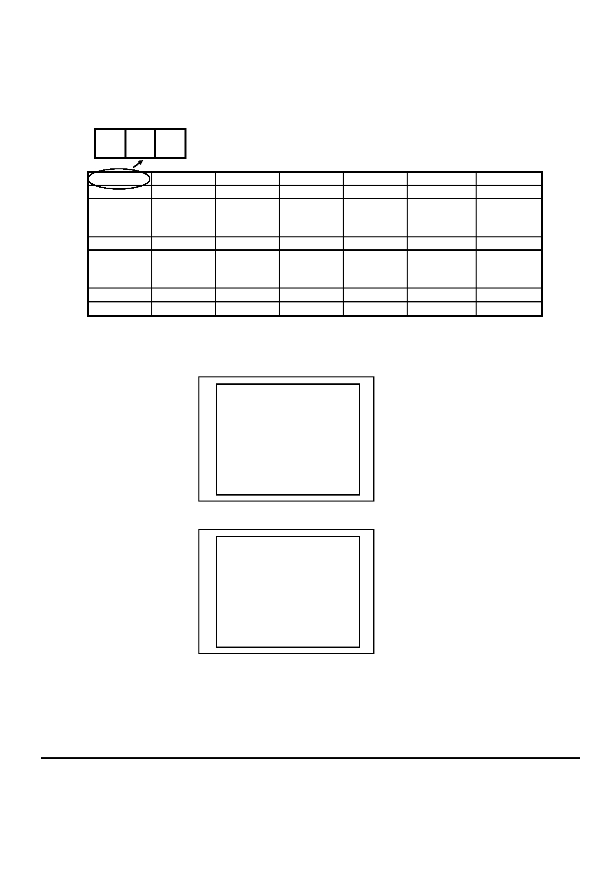
6.4.3 262,144 colors
This product can display 262,144 colors with 64 gray scales by combination ② .
(See " 6.4.1 Combinations of input data signals and FRC signal ".)
Also the relation between display colors and input data signals is as follows.
Data signal (0: Low level, 1: High level)
Display colors
R5 R4 R3 R2 R1 R0 G5 G4 G3 G2 G1 G0 B 5 B 4 B 3 B 2 B 1 B 0
Black
0
0
0
0
0
0
0
0
0
0
0
0
0
0
0
0
0
0
Blue
0
0
0
0
0
0
0
0
0
0
0
0
1
1
1
1
1
1
Red
1
1
1
1
1
1
0
0
0
0
0
0
0
0
0
0
0
0
Magenta 1
1
1
1
1
1
0
0
0
0
0
0
1
1
1
1
1
1
Green
0
0
0
0
0
0
1
1
1
1
1
1
0
0
0
0
0
0
Cyan
0
0
0
0
0
0
1
1
1
1
1
1
1
1
1
1
1
1
Yellow
1
1
1
1
1
1
1
1
1
1
1
1
0
0
0
0
0
0
White
1
1
1
1
1
1
1
1
1
1
1
1
1
1
1
1
1
1
Black
0
0
0
0
0
0
0
0
0
0
0
0
0
0
0
0
0
0
0
0
0
0
0
1
0
0
0
0
0
0
0
0
0
0
0
0
dark
0
0
0
0
1
0
0
0
0
0
0
0
0
0
0
0
0
0
:
:
:
:
:
:
bright
1
1
1
1
0
1
0
0
0
0
0
0
0
0
0
0
0
0
1
1
1
1
1
0
0
0
0
0
0
0
0
0
0
0
0
0
Red
1
1
1
1
1
1
0
0
0
0
0
0
0
0
0
0
0
0
Black
0
0
0
0
0
0
0
0
0
0
0
0
0
0
0
0
0
0
0
0
0
0
0
0
0
0
0
0
0
1
0
0
0
0
0
0
dark
0
0
0
0
0
0
0
0
0
0
1
0
0
0
0
0
0
0
:
:
:
:
:
:
bright
0
0
0
0
0
0
1
1
1
1
0
1
0
0
0
0
0
0
0
0
0
0
0
0
1
1
1
1
1
0
0
0
0
0
0
0
Green
0
0
0
0
0
0
1
1
1
1
1
1
0
0
0
0
0
0
URL: www.topwaydisplay.com
Document Name: LMT150FNGFSA-Manual-Rev0.1.DOC
Page 19 of 30

TOPWAY
LCD Module User Manual
LMT150FNGFSA
-
Black
0
0
0
0
0
0
0
0
0
0
0
0
0
0
0
0
0
0
0
0
0
0
0
0
0
0
0
0
0
0
0
0
0
0
0
1
dark
0
0
0
0
0
0
0
0
0
0
0
0
0
0
0
0
1
0
:
:
:
:
:
:
bright
0
0
0
0
0
0
0
0
0
0
0
0
1
1
1
1
0
1
0
0
0
0
0
0
0
0
0
0
0
0
1
1
1
1
1
0
Blue
0
0
0
0
0
0
0
0
0
0
0
0
1
1
1
1
1
1
URL: www.topwaydisplay.com
Document Name: LMT150FNGFSA-Manual-Rev0.1.DOC
Page 20 of 30
TOPWAY
LCD Module User Manual
LMT150FNGFSA
-
6.5 DISPLAY POSITIONS
The following table is the coordinates per pixel (See "6.6 SCANNING DIRECTIONS" .).
C (0, 0)
B
G
R
C( 0, 0)
C( 1, 0)
∙ ∙ ∙
C( X, 0)
∙ ∙ ∙
C(1022, 0)
C(1023, 0)
C( 0, 1)
C( 1, 1)
∙ ∙ ∙
C( X, 1)
∙ ∙ ∙
C(1022, 1)
C(1023, 1)
∙
∙
∙
∙
∙
∙
∙
∙
∙
∙ ∙ ∙
∙
∙ ∙ ∙
∙
∙ ∙ ∙
∙
∙
∙
∙
∙
∙
∙
C( 0, Y)
C( 1, Y)
∙ ∙ ∙
C( X, Y)
∙ ∙ ∙
C(1022, Y)
C(1023, Y)
∙
∙
∙
∙
∙
∙
∙
∙
∙
∙ ∙ ∙
∙
∙ ∙ ∙
∙
∙
∙
∙
∙
∙
∙
∙
∙
C( 0, 766)
C( 1, 766)
∙ ∙ ∙
C( X, 766)
∙ ∙ ∙
C(1022, 766)
C(1023, 766)
C( 0, 767)
C( 1, 767)
∙ ∙ ∙
C( X, 767)
∙ ∙ ∙
C(1022, 767)
C(1023, 767)
6.6 SCANNING DIRECTIONS
The following figures are seen from a front view.
C (0, 0)
C (1023, 0)
D (0, 0)
D (1023, 0)
TOPWAY
Note1
C (0, 767)
C (1023, 767)
D (0, 767)
D (1023, 767)
Figure1. Normal scan (DPS: Low or Open)
C (0, 0)
D Y A76 7) W P D O(0, 7 67)
C (1023, 0)
(1023,
T
Note1
C (0, 767)
C (1023, 767)
D (1023, 0)
D (0, 0)
Figure2. Reverse scan (DPS: High)
Note1: Meaning of C (X, Y) and D (X, Y)
C (X, Y): The coordinates of the display position (See " 6.5 DISPLAY POSITIONS ".)
D (X, Y): The data number of input signal for LCD panel signal processing board
URL: www.topwaydisplay.com
Document Name: LMT150FNGFSA-Manual-Rev0.1.DOC
Page 21 of 30
TOPWAY
LCD Module User Manual
LMT150FNGFSA
-
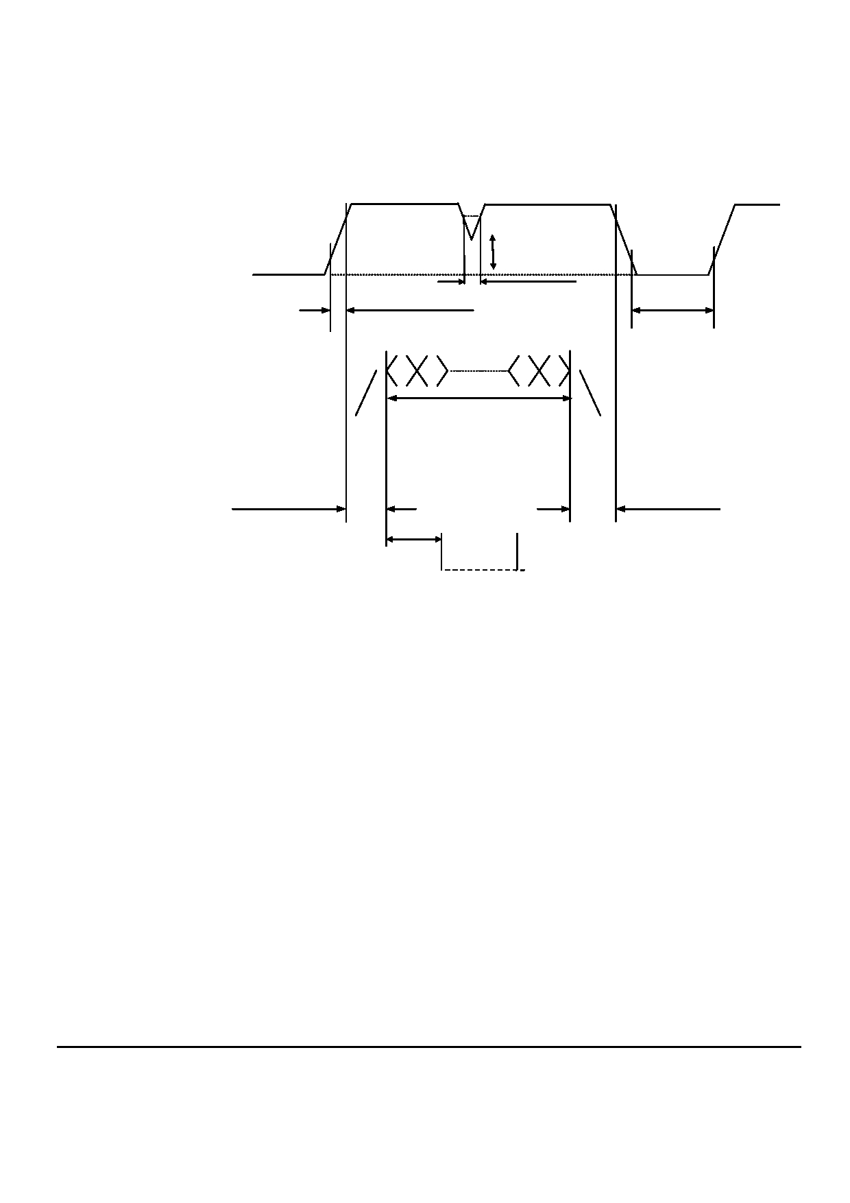
6.7 Power On/Off Sequence
6.7.1 LCD panel signal processing board
ON
OFF
ON
0.9VCC
0.9VCC
VCC
Note1
0.1VCC
0V
2.7V
0.1VCC
0.5ms < t1 < 10ms
VCC dip < 10ms
t2>1000ms
Display signals*
VALID period
Function signals
0V
Note2
0.5ms < t3 < 50ms
0ms < t4 < 50ms
t5 ≥ 200ms (Recommended value)
Turn-on
Backlight signal
period
Note3
* These signals should be measured at the terminal of 100 resistances.
Note1: If there is a voltage variation (voltage drop) at the rising edge of VCC below 3.0V,
there is a possibility that a product does not work due to a protection circuit.
Note2: Display signals (D0+/-, D1+/-, D2+/-, D3+/- and CLK+/-) and function signals (DPS
and FRC) must be set to Low or High-impedance, except the VALID period (See
above sequence diagram), in order to avoid the circuitry damage.
If some of display and function signals of this product are cut while this product is
working, even if the signal input to it once again, it might not work normally. If a
customer stops the display and function signals, VCC also must be shut down.
Note3: In order to avoid unstable data display, the backlight is recommended to turn on within
the VALID period of display. Recommended value: t5 ≥ 200ms.
URL: www.topwaydisplay.com
Document Name: LMT150FNGFSA-Manual-Rev0.1.DOC
Page 22 of 30
TOPWAY
LCD Module User Manual
LMT150FNGFSA
-
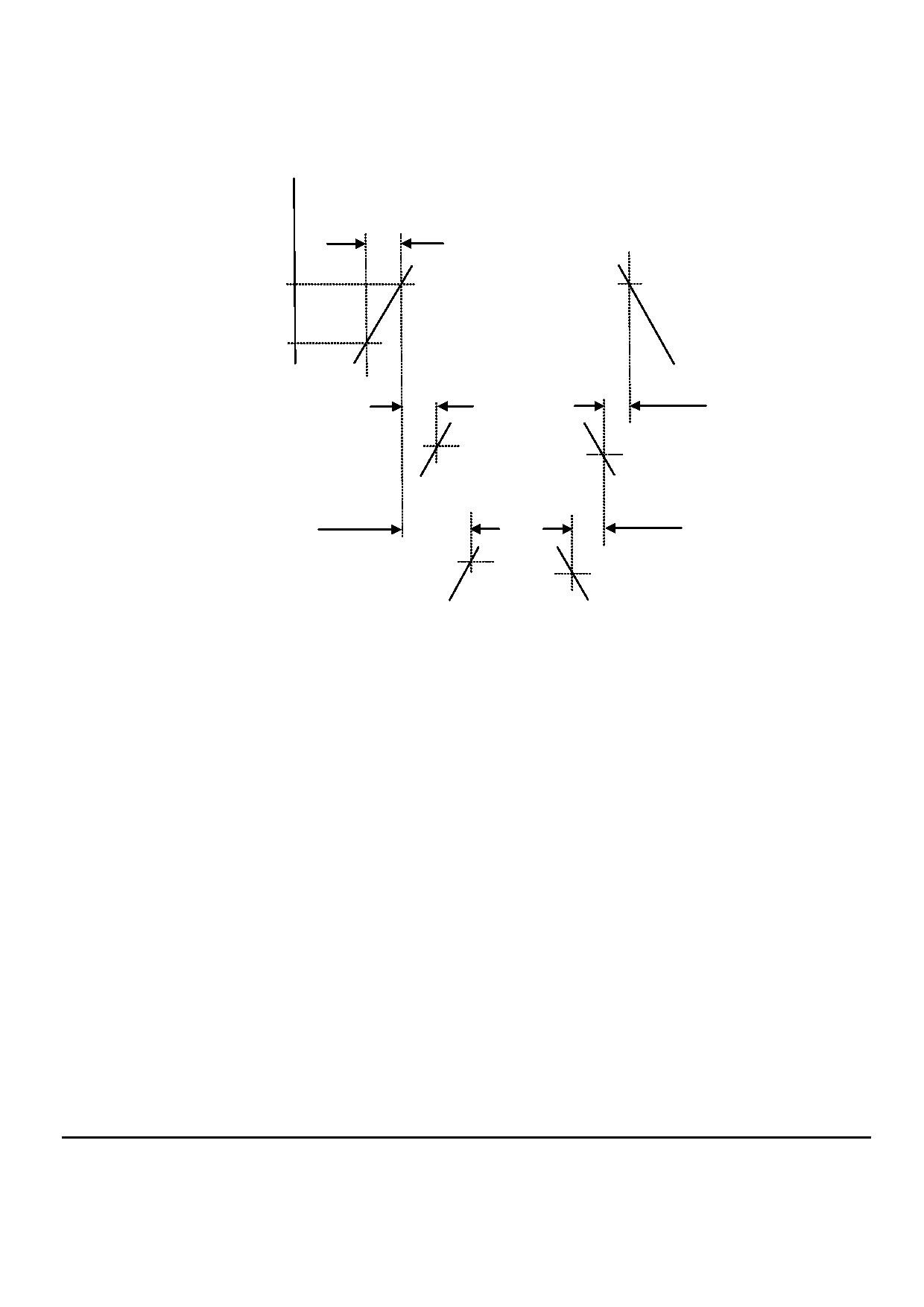
6.7.2 LED driver board
Voltage
0.5ms < t1 < 50ms
ON
OFF
VDD
0.9VDD
0.9VDD
0.1VDD
0V
Time
10ms < t2
0ms < t3
PWM
1.2V
0.35V
20ms < t4
0ms < t5
1.5V
BRTC
0.8V
Note1: These are the display and function signals for LCD panel signal processing board.
URL: www.topwaydisplay.com
Document Name: LMT150FNGFSA-Manual-Rev0.1.DOC
Page 23 of 30
TOPWAY
LCD Module User Manual
LMT150FNGFSA
-
7.
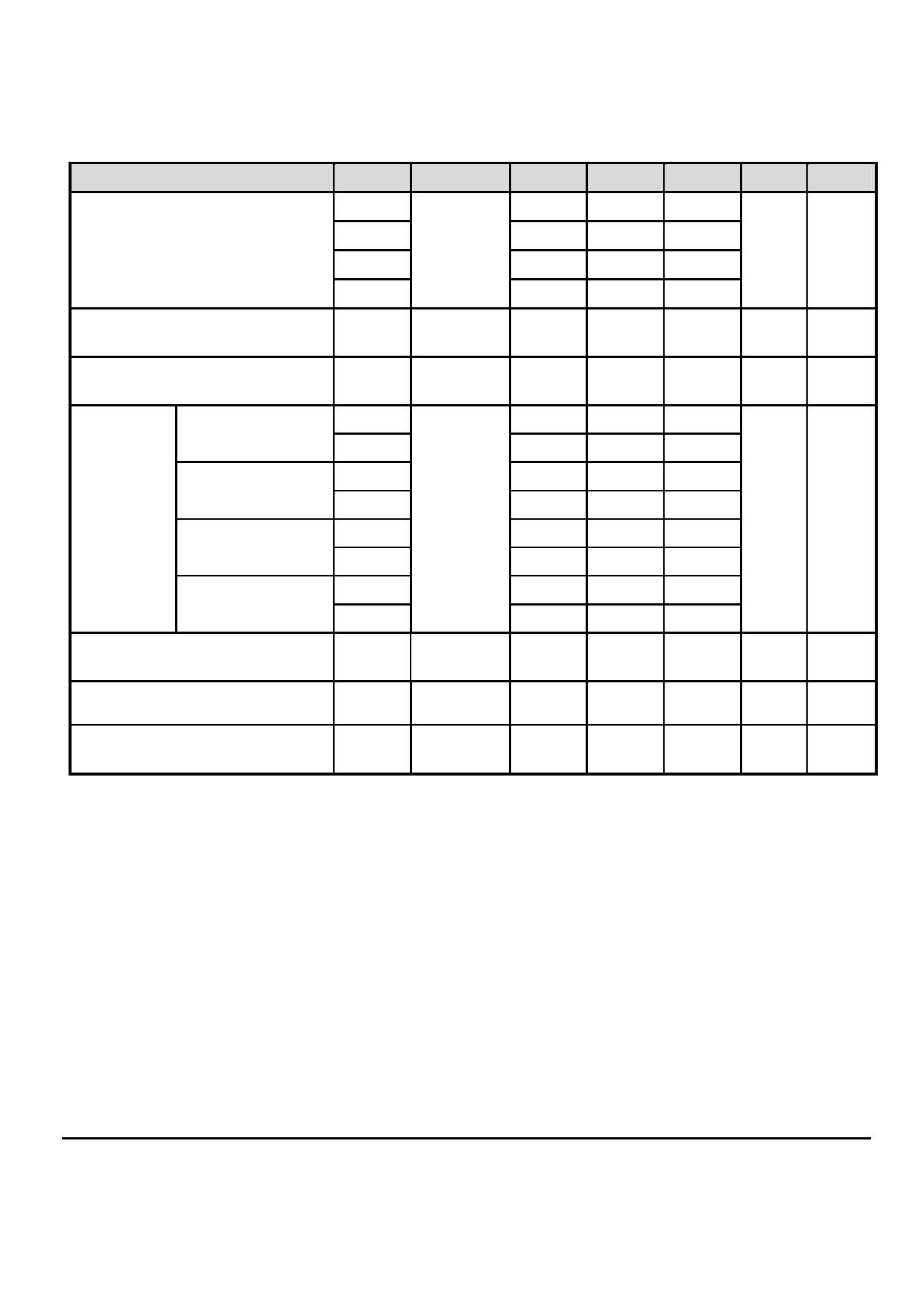
Optical Characteristics
Ta=25 ℃
Item
Symbol Condition
Min
Typ
Max
Unit
Remark
θ T
80
89
-
θ B
80
89
-
View Angles
CR ≧ 10
Degree
Note 2
θL
80
89
-
θR
80
89
-
Note1
Contrast Ratio
CR
θ=0 °
600
1000
-
-
Note3
Note1
Response Time
T ON +T OFF
25 ℃
-
25
40
ms
Note4
x
0.267
0.317
0.367
White
y
0.311
0.361
0.411
x
0.594
0.644
0.694
Red
y
0.291
0.341
0.391
Note5
Chromaticity
Backlight is
-
x
on
0.258
0.308
0.358
Note1
Green
y
0.575
0.625
0.675
x
0.099
0.149
0.199
Blue
y
0.030
0.080
0.130
Note1
Uniformity
U
70
75
%
Note6
NTSC
-
65
72
%
Note 5
Note1
Luminance
L
1500
1700
-
cd/m
2
Note7
Test Conditions:
1. The ambient temperature is 25±2 ℃ .humidity is 65±7%. PWM duty ratio is 100%.
2. The test systems refer to Note 1 and Note 2.
3. Contrast Ratio, Chromaticity, Uniformity, and Luminance is measured by SR-UL, SR-3AR or
equivalent.
4. Response Time is measured by TRD-100, LCD-5200 or equivalent.
URL: www.topwaydisplay.com
Document Name: LMT150FNGFSA-Manual-Rev0.1.DOC
Page 24 of 30
TOPWAY
LCD Module User Manual
LMT150FNGFSA
-
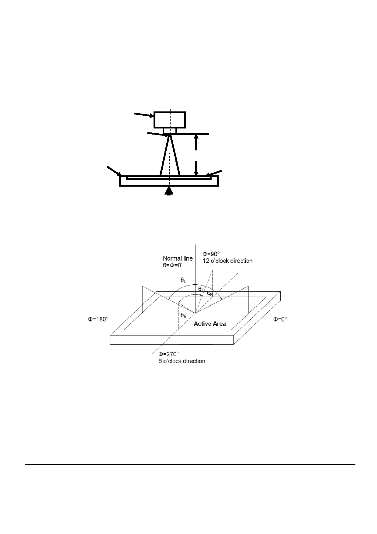
Note 1: Definition of optical measurement system.
The optical characteristics should be measured in dark room. After 20 minutes operation, the
optical properties are measured at the center point of the LCD screen. All input terminals LCD
panel must be ground when measuring the center area of the panel.
Photo detector
Field
500mm
TFT-LCD Module
LCD Panel
The center of the screen
Note 2: Definition of viewing angle range and measurement system.
Viewing angle is measured at the center point of the LCD by LCD5200
Fig. 1 Definition of viewing angle
URL: www.topwaydisplay.com
Document Name: LMT150FNGFSA-Manual-Rev0.1.DOC
Page 25 of 30
TOPWAY
LCD Module User Manual
LMT150FNGFSA
-
Note 3: Definition of contrast ratio
The contrast ratio is calculated by using the following formula.
Contrast ratio (CR) =
Luminance of white screen
Luminance of black screen
Note 4: Definition of Response time
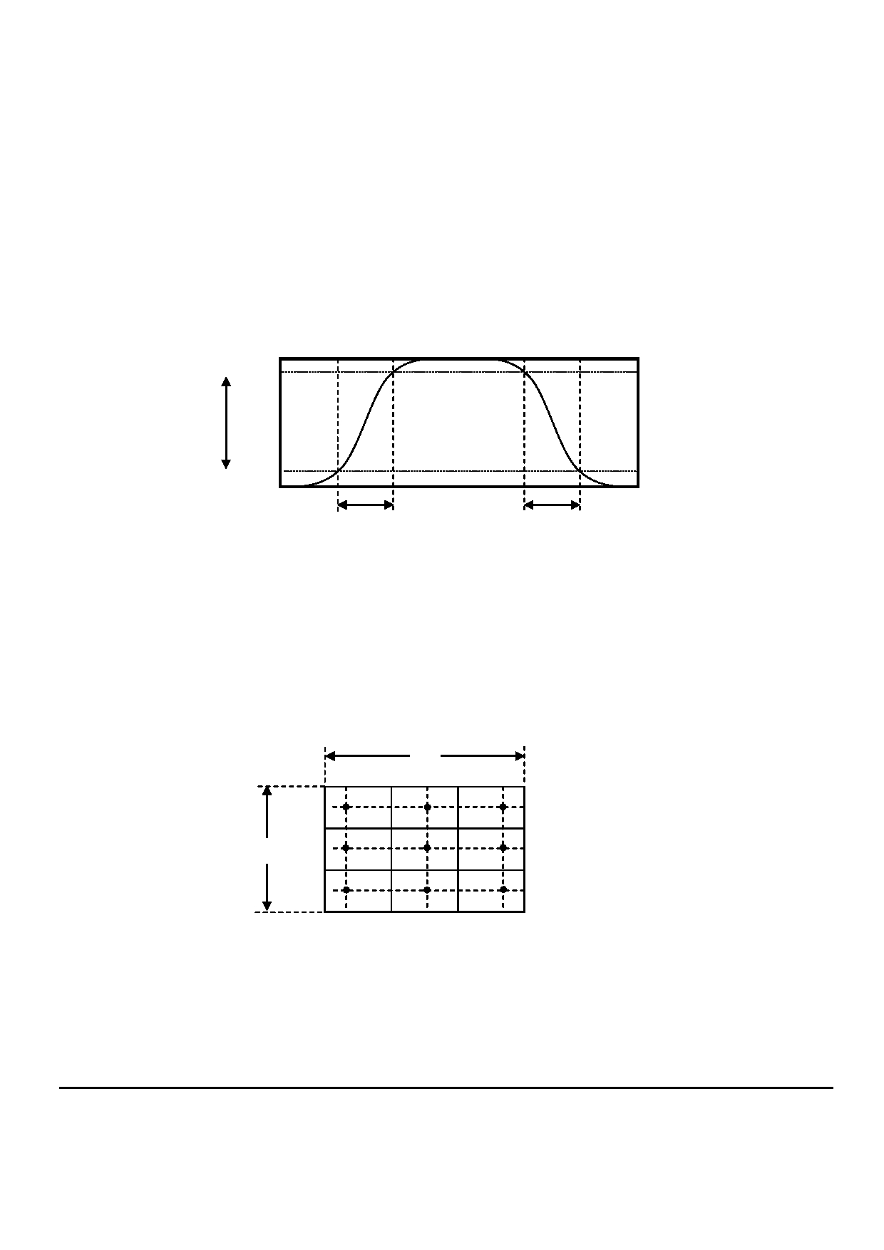
The response time is defined as the LCD optical switching time interva l between “ Black ” state
a nd “ White ” st ate. Rise time (Ton) is the time between photo detector output intensity changed
from 10% to 90%. And fall time (Toff) is the time between photo detector output intensity
changed from 90% to 10%.
Product surface temperature: TopF= 29 ℃ .
100%
White
90%
Luminance
Black
10%
0%
Ton
Toff
Note 5: Definition of color chromaticity (CIE1931)
Color coordinates measured at center point of LCD.
Note 6: Definition of Luminance Uniformity
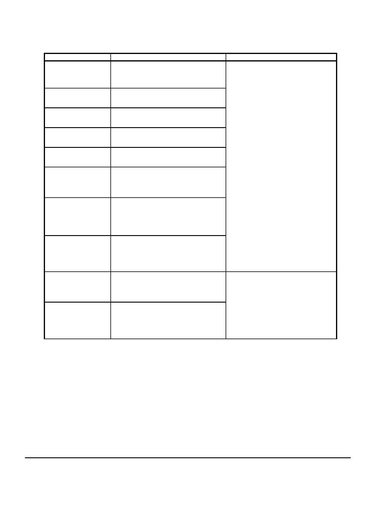
Active area is divided into 9 measuring areas (Refer Fig. 2). Every measuring point is placed at
the center of each measuring area.
Luminance Uniformity(U) = Lmax/ Lmin
H-------Active area length V----- Active area width
H
H/10
H/2
H/10
②
③
V/10
①
④
⑤
⑥
V
V/2
D
⑦
⑧
⑨
V/10
Fig. 2 Definition of uniformity
Lmax: The measured maximum luminance of all measurement position
Lmin: The measured minimum luminance of all measurement position.
Note 7: Definition of Luminance
Measure the luminance of white state at center point.
URL: www.topwaydisplay.com
Document Name: LMT150FNGFSA-Manual-Rev0.1.DOC
Page 26 of 30
TOPWAY
LCD Module User Manual
LMT150FNGFSA
-
8.
Environmental / Reliability Test
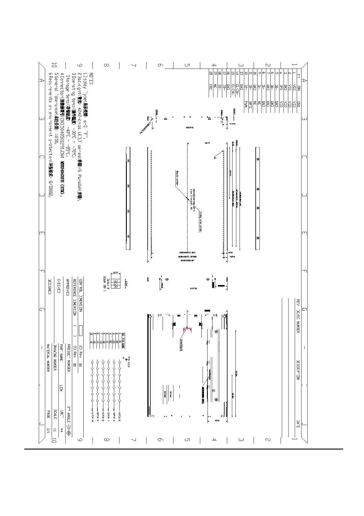
Test item
Condition
Judgment
Note1
High temperature and
① 60 2 C, RH= 90%, 240hours
humidity
(Operation)
② Display data is white.
High temperature
① 70 3 C, 240hours
(Operation)
② Display data is white.
High temperature
① 85 3 C, 240hours
(Storage)
② Display data is white.
Low temperature
① -30 3 C, 240hours
(Operation)
② Display data is white.
Low temperature
① -40 3 C, 240hours
(Storage)
② Display data is white.
No display malfunctions
① -20 3 C 1hour
Heat cycle
70 3 C 1hour
(Operation)
② 50cycles, 4hours/cycle
③ Display data is white.
① -40 3 C, 30minutes
80 3 C, 30minutes
Thermal shock
(Non operation)
② 100cycles, 1hour/cycle
③ Temperature transition time is within 5
minutes.
① 150pF, 150 , Air:
8kV contact:
ESD
4kV
(Operation)
② 5 places ( Edge&Center ) Note2
③
5 times each places at 1 sec interval
① 5 to 100Hz, 11.76m/s 2
Vibration
② 1 minute/cycle
(Non operation)
③ X, Y, Z directions
④ 50 times each directions
No display malfunctions
No physical damages
① 294m/s 2 , 11ms
Mechanical shock
(Non operation)
② X, Y, Z directions
③ 3 times each directions
Note1: Display and appearance are checked under environmental conditions equivalent to the
inspection conditions of defect criteria.
URL: www.topwaydisplay.com
Document Name: LMT150FNGFSA-Manual-Rev0.1.DOC
Page 27 of 30
TOPWAY
LCD Module User Manual
LMT150FNGFSA
-
9.
Mechanical drawing
URL: www.topwaydisplay.com
Document Name: LMT150FNGFSA-Manual-Rev0.1.DOC
Page 28 of 30

TOPWAY
LCD Module User Manual
LMT150FNGFSA
-
10. Precautions for Use of LCD Modules
10.1 Handling Precautions
10.1.1 The display panel is made of glass. Do not subject it to a mechanical shock by dropping it from a
high place, etc.
10.1.2 If the display panel is damaged and the liquid crystal substance inside it leaks out, be sure not to
get any in your mouth, if the substance comes into contact with your skin or clothes, promptly
wash it off using soap and water.
10.1.3 Do not apply excessive force to the display surface or the adjoining areas since this may cause
the color tone to vary.
10.1.4 The polarizer covering the display surface of the LCD module is soft and easily scratched.
Handle this polarizer carefully.
10.1.5 If the display surface is contaminated, breathe on the surface and gently wipe it with a soft dry
cloth. If still not completely clear, moisten cloth with one of the following solvents:
- Isopropyl alcohol
- Ethyl alcohol
Solvents other than those mentioned above may damage the polarizer. Especially, do not use
the following:
- Water
- Ketone
- Aromatic solvents
10.1.6 Do not attempt to disassemble the LCD Module.
10.1.7 If the logic circuit power is off, do not apply the input signals.
10.1.8 To prevent destruction of the elements by static electricity, be careful to maintain an optimum
work environment.
10.1.8.1 Be sure to ground the body when handling the LCD Modules.
10.1.8.2 Tools required for assembly, such as soldering irons, must be properly ground.
10.1.8.3 To reduce the amount of static electricity generated, do not conduct assembly and other work
under dry conditions.
10.1.8.4 The LCD Module is coated with a film to protect the display surface. Be care when peeling off
this protective film since static electricity may be generated.
10.2 Storage Precautions
10.2.1 When storing the LCD modules, avoid exposure to direct sunlight or to the light of fluorescent
lamps.
10.2.2 The LCD modules should be stored under the storage temperature range. If the LCD modules
will be stored for a long time, the recommend condition is:
Temperature : 0 ℃ ~ 40 ℃
Relatively humidity: ≤80%
10.2.3 The LCD modules should be stored in the room without acid, alkali and harmful gas.
10.3 Transportation Precautions
The LCD modules should be no falling and violent shocking during transportation, and also should
avoid excessive press, water, damp and sunshine.
URL: www.topwaydisplay.com
Document Name: LMT150FNGFSA-Manual-Rev0.1.DOC
Page 30 of 30