
SHANGHAI AVIC OPTOELECTRONICS
Model No.TM121TDSG02
MODEL NO :
TM121TDSG02
MODEL VERSION:
00
SPEC VERSION :
1.0
ISSUED DATE:
2015-12-22
■Preliminary Specification
□Final Product Specification
Customer :
Approved by
Notes
TIANMA Confirmed :
Prepared by
Checked by
Approved by
Xianchen.Fu
Fan.Jiang
Feng.Qin
This technical specification is subjected to change without notice
URL: www.topwaydisplay.com
Page 1 of 32

SHANGHAI AVIC OPTOELECTRONICS
Model No.TM121TDSG02
TABLE OF CONTENTS
1. OUTLINE ........................................................................................................................................................................ 4
2. GENERAL SPECIFICATIONS .................................................................................................................................... 5
3. BLOCK DIAGRAM ....................................................................................................................................................... 6
4. DETAILED SPECIFICATIONS ................................................................................................................................... 7
5. ESTIMATED LUMINANCE LIFETIME .................................................................................................................. 26
6. RELIABILITY TESTS ................................................................................................................................................ 27
7. MARKINGS .................................................................................................................................................................. 28
8. PACKING, TRANSPORTATION AND DELIVERY ............................................................................................... 29
9. PRECAUTIONS ........................................................................................................................................................... 30
10. OUTLINE DRAWINGS ............................................................................................................................................. 32
URL: www.topwaydisplay.com
Page 2 of 32

SHANGHAI AVIC OPTOELECTRONICS
Model No.TM121TDSG02
RECORD OF REVISION
Rev
Issued Date
Description
Editor
1.0
2015-12-22
Preliminary Specification Release
Xianchen Fu
URL: www.topwaydisplay.com
Page 3 of 32

SHANGHAI AVIC OPTOELECTRONICS
Model No.TM121TDSG02
1. OUTLINE
1.1 STRUCTURE AND PRINCIPLE
Color LCD module TM121TDSG02-00 is composed of the amorphous silicon thin film transistor
liquid crystal display (a-Si TFT LCD) panel structure with driver LSIs for driving the TFT (Thin Film
Transistor) array and a backlight.
The a-Si TFT LCD panel structure is injected liquid crystal material into a narrow gap between the
TFT array glass substrate and a color-filter glass substrate.
Color (Red, Green, Blue) data signals from a host system (e.g. signal generator, etc.) are modulated
into best form for active matrix system by a signal processing board, and sent to the driver LSIs which
drive the individual TFT arrays.
The TFT array as an electro-optical switch regulates the amount of transmitted light from the
backlight assembly, when it is controlled by data signals. Color images are created by regulating the
amount of transmitted light through the TFT array of red, green and blue dots.
1.2 APPLICATION
For industrial use
1.3 FEATURES
High luminance
High contrast
Wide viewing angle
Fast response time
LVDS interface
Selectable 8-bit or 6-bit digital signals for data of RGB
Reversible-scan direction
Built in LED driver
Replaceable lamp for backlight
URL: www.topwaydisplay.com
Page 4 of 32

SHANGHAI AVIC OPTOELECTRONICS
Model No.TM121TDSG02
2. GENERAL SPECIFICATIONS
Display area
245.76 (H) 184.32 (V) mm
Diagonal size of display
31cm (12.1 inches)
Drive system
a-Si TFT active matrix
16,194,277 colors (At 8-bit input, FRC terminal= High)
Display color
262,144 colors (At 6-bit input, FRC terminal= Low or Open)
Pixel
1,024 (H) 768 (V) pixels
Pixel arrangement
BGR (Blue dot, Green dot, Red dot) vertical stripe
Dot pitch
0.080 (H) 0.240 (V) mm
Pixel pitch
0.240 (H) 0.240 (V) mm
Module size
279.0 (W) 209.0 (H) 8.6 (D) mm (typ.)
Weight
485g
Contrast ratio
700:1 (typ.)
At the contrast ratio 10:1
Viewing angle
Horizontal: Right side 80 (typ.), Left side 80 (typ.)
Vertical: Up side 80 (typ.), Down side 80 (typ.)
At DPS= Low or Open: Normal scan
Viewing direction without image reversal: Up side (12 o'clock)
Designed viewing direction
Viewing direction with contrast peak: Down side (6 o'clock)
Viewing angle with optimum grayscale (
≒ 2.2): Normal axis
(perpendicular)
(source IC location is 12 o'clock)
Polarizer surface
Antiglare
Polarizer pencil-hardness
3H (min.) [by JIS K5600]
At LCD panel center
Color gamut
55% (typ.) [against NTSC color space]
Ton+Toff (10% 90%)
Response time
8ms (typ.)
At the maximum luminance control
Luminance
450cd/m (typ.)
2
Signal system
LVDS 1port
LCD panel signal processing board: 3.3V
Power supply voltage
LED driver: 12.0V
Backlight
LED backlight built in LED driver
At the maximum luminance control, Checkered flag pattern
Power consumption
6.4 W (typ.)
URL: www.topwaydisplay.com
Page 5 of 32

SHANGHAI AVIC OPTOELECTRONICS
Model No.TM121TDSG02
3. BLOCK DIAGRAM
Host
LCD module (Product)
D0+
100
D0-
LCD panel
D1+
100
D1-
H: 1,024 × 3 (R, G, B)
V: 768
D2+
100
D2-
D3+
100
D3-
CLK+
100
CLK-
DPS
FRC
768 lines
Power supply
for gradation
V-driver
GND
Note1
Note2
Fuse
DC/DC
VCC
converter
Fuse
VDD
PWM
BRTC
LED driver
LED Backlight
GND
LCD panel signal processing board
FG
Note1: Relations between GND (Signal ground and LED driver ground) and FG (Frame ground) in the
LCD module are as follows.
GND- FG
Connected
Note2: GND and FG must be connected to customer equipment’s ground, and it is recommended that
these grounds to be connected together in customer equipment.
URL: www.topwaydisplay.com
Page 6 of 32

SHANGHAI AVIC OPTOELECTRONICS
Model No.TM121TDSG02
4. DETAILED SPECIFICATIONS
4.1 MECHANICAL SPECIFICATIONS
Parameter
Specification
Unit
Module size
279.0 0.5 (W) 209.0 0.5 (H) 8.6 0.5(D)
Note1
mm
Display area
245.76 (H) 184.32 (V)
Note1
mm
Weight
483 (typ.),
g
Note1: See " 10. OUTLINE DRAWINGS ".
4.2 ABSOLUTE MAXIMUM RATINGS
GND=0V
Parameter
Symbol
Rating
Unit
Remarks
Power supply
LCD panel signal processing board
VCC
-0.3 to +3.96
V
voltage
LED driver
VDD
-0.3 to +15.0
Display signals
VD
-0.5 to 3.96
Note1
V
Function signals
Input voltage for
VF
-0.5 to 3.96
Note2
signals
PWM
-0.3 to +15.0
V
Function signal for LED driver
BRTC
-0.3 to +15.0
V
Operating Temperature
Top
-20 to +70
C
Storage temperature
Tst
-30 to +80
C
-
≤ 95
%
Ta ≤ 40 C
≤ 85
%
40 C < Ta ≤ 50 C
Relative Humidity
Note3
RH
≤ 55
%
50 C < Ta ≤ 60
C
≤ 36
%
60 C < Ta ≤ 70 C
≤ 24
%
70 C < Ta ≤ 80 C
Absolute Humidity
AH
≤ 70
Ta > 70 C
Note1: D0+/-, D1+/-, D2+/-, D3+/- and CLK+/-
Note2: DPS and FRC
Note3: Ta means the ambient temperature.
It is necessary to limit the relative humidity to the specified temperature range.
Condensation on the module is not allowed.
URL: www.topwaydisplay.com
Page 7 of 32
SHANGHAI AVIC OPTOELECTRONICS
Model No.TM121TDSG02
4.3.2 LED driver
(Ta= 25 C)
Parameter
Symbol
min.
typ.
max.
Unit
Remarks
Power supply voltage
VDD
10.8
12.0
13.2
V
Note1
480
At the maximum
Power supply current
IDD
-
410
Note2
mA
luminance control
for VDD
Permissible ripple voltage
VRPD
-
-
200
mVp-p
Note3
Input voltage for
High
VDFH1
2.0
-
VDD
V
-
PWM signal
Low
VDFL1
0
-
0.8
V
Input voltage for
High
VDFH2
2.0
-
VDD
V
-
BRTC signal
Low
VDFL2
0
-
0.8
V
PWM frequency
f PWM
200
-
20k
Hz
Note4, Note5
PWM duty ratio
DR PWM
1
-
100
%
Note6, Note7
PWM pulse width
tPWH
5
-
-
s
Note1: When designing of the power supply, take the measures for the prevention of surge voltage.
Note2: This value excludes peak current such as overshoot current.
Note3: The power supply lines (VDD and GND) may have ripple voltage during luminance control
of LED. There is the possibility that the ripple voltage produces acoustic noise and signal
wave noise in audio circuit and so on. Put a capacitor between the power supply lines (VDD
and GND) to reduce the noise if necessary.
Note4: A recommended f PWM value is as follows.
2n 1
f PWM
fv
4
frame frequency of LCD module)
Note5: Depending on the frequency used, some noise may appear on the screen, please conduct a
thorough evaluation.
Note6: While the BRTC signal is high, do not set the tPWH (PWM pulse width) is less than 5 s . It
may cause abnormal working of the backlight. In this case, turn the backlight off and then on
again by BRTC signal.
Note7: Regardless of the PWM frequency, both PWM duty ratio and PWM pulse width must be
always more than the minimum values.
URL: www.topwaydisplay.com
Page 9 of 32

SHANGHAI AVIC OPTOELECTRONICS
Model No.TM121TDSG02
4.3.3 Power supply voltage ripple
This product works if the ripple voltage levels are over the permissible values as the following table,
but there might be noise on the display image.
Ripple voltage
Note1
Power supply voltage
Unit
(Measure at input terminal of power supply)
VCC
3.3V
300
mVp-p
VDD
12.0V
200
mVp-p
Note1: The permissible ripple voltage includes spike noise.
4.3.4 Fuse
Fuse
Parameter
Rating
Fusing current
Remarks
Type
Supplier
KAMAYA ELECTRIC
1.5A
VCC
FCC16152AB
3.0A
Co., Ltd.
36V
Note1
KAMAYA ELECTRIC
1.5A
VDD
FCC16152AB
3.0A
Co., Ltd.
36V
Note1: The power supply’s rated current must be more than the fusing current. If it is less than the
fusing current, the fuse may not blow in a short time, and then nasty smell, smoke and so on
may occur.
URL: www.topwaydisplay.com
Page 10 of 32
SHANGHAI AVIC OPTOELECTRONICS
Model No.TM121TDSG02
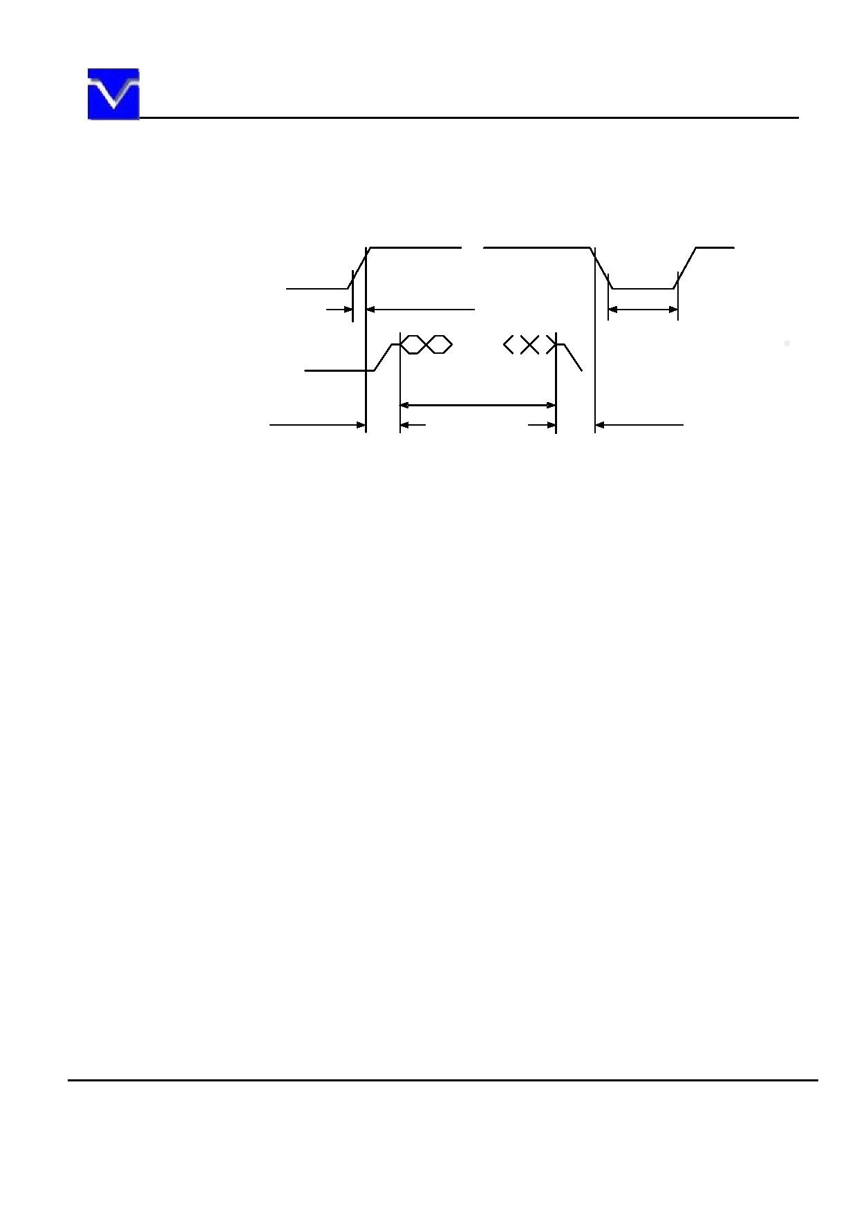
4.4 POWER SUPPLY VOLTAGE SEQUENCE
4.4.1 LCD panel signal processing board
ON
OFF
ON
VCC
0.9VCC
0.9VCC
Note1
0.1VCC
0.1VCC
0V
0.5ms Tr < 10ms
Toff 1000ms
Display signals*
Function signals
0V
Note2
VALID period
0.5ms < t < 50ms
0ms < t < 50ms
* These signals should be measured at the terminal of 100 resistance.
Note1: If there is a voltage variation (voltage drop) at the rising edge of VCC below 3.0V, there is a
possibility that a product does not work due to a protection circuit.
Note2: Display signals (D0+/-, D1+/-, D2+/-, D3+/- and CLK+/-) and function signals (DPS and
FRC) must be set to Low or High-impedance, except the VALID period (See above sequence
diagram), in order to avoid the circuitry damage.
If some of display and function signals of this product are cut while this product is working,
even if the signal input to it once again, it might not work normally. If a customer stops the
display and function signals, VCC also must be shut down.
URL: www.topwaydisplay.com
Page 11 of 32
SHANGHAI AVIC OPTOELECTRONICS
Model No.TM121TDSG02
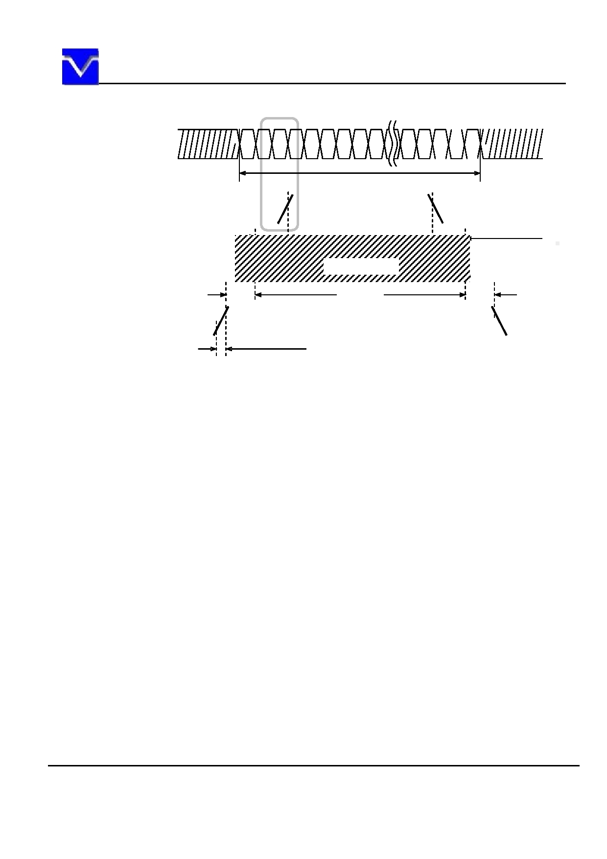
4.4.2 LED driver
Note2
Display signals
Function signals
Note1
VALID period
2.0V
2.0V
BRTC
10ms < Tr
0ms < Tf
PWM
2.0V
VALID period
2.0V
10ms < Tr
0ms < Tf
0.9VDD
0.9VDD
VDD
0.1VDD
0.5ms < Tr < 50ms
Note1: These are the display and function signals for LCD panel signal processing board.
Note2: The backlight should be turned on within the valid period of display and function signals, in
order to avoid unstable data display.
URL: www.topwaydisplay.com
Page 12 of 32

SHANGHAI AVIC OPTOELECTRONICS
Model No.TM121TDSG02
4.5 CONNECTIONS AND FUNCTIONS FOR INTERFACE PINS
4.5.1 LCD panel signal processing board
CN1 socket (LCD module side): MSB240420HE (STM)
Adaptable plug:
P240420 (STM) or DF14-20S-1.25C (Hirose Electric Co., Ltd. (HRS))
Pin No.
Symbol
Signal
Input data signal: 8-bit
Input data signal: 6-bit
Remarks
1
VCC
Power supply
Power supply
Note1
2
VCC
3
GND
Ground
Ground
Note1
Selection of the
4
FRC
High
Low or Open
Note2, Note3
number of colors
5
D0-
Pixel data
R0-R5, G0
Note4
6
D0+
7
GND
Ground
Ground
Note1
8
D1-
Pixel data
G1-G5, B0-B1
Note4
9
D1+
10
GND
Ground
Ground
Note1
11
D2-
Pixel data
B2-B5, DE
Note4
12
D2+
13
GND
Ground
Ground
Note1
14
CLK-
Pixel clock
Pixel clock
Note4
15
CLK+
16
GND
Ground
Ground
Note1
D3-
17
R6-R7
/ GND
Pixel data
G6-G7
Ground
Note4
D3+
/ Ground
18
B6-B7
/ GND
Selection
High:
Reverse scan
19
DPS
Note5
of scan direction
Low or Open:
Normal scan
20
N.C.
Non connection
-
Keep this pin Open.
Note1: All GND and VCC terminals should be used without any non-connected lines.
Note2: See " 4.6 DISPLAY COLORS AND INPUT DATA SIGNALS ".
Note3: See " 4.5.4 Connection between receiver and transmitter for LVDS ".
Note4: Twist pair wires with 100 (Characteristic impedance) should be used between LCD panel
signal processing board and LVDS transmitter.
Note5: See " 4.8 SCANNING DIRECTIONS ".
URL: www.topwaydisplay.com
Page 13 of 32
SHANGHAI AVIC OPTOELECTRONICS
Model No.TM121TDSG02
4.5.2 LED driver
CN2 socket (LCD module side): MSB24038P5 (STM)
Adaptable plug:
P24038P5 (STM) or 51146-0500 (Molex)
Pin No.
Symbol
Signal
Remarks
1
N. C.
Non connection
Keep this pin Open.
2
PWM
Luminance control
PWM Dimming
3
BRTC
Backlight ON/OFF control
High: ON / Low: OFF
4
GND
Ground
-
5
VDD
Power supply
-
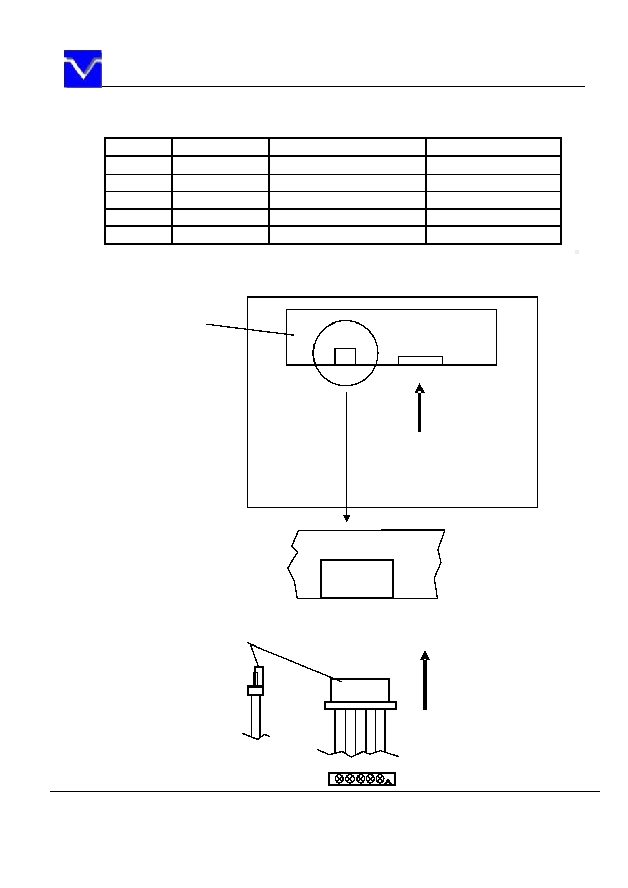
4.5.3 Positions of plug and socket
Rear side
LCD panel signal
processing board
CN2
CN1
5
1
20
1
Insert direction
LCD panel signal
processing board
CN2 socket: MSB24038P5
CN2
5 4 3 2 1
Adaptable plug: P24038P5 or
51146-0500
Insert direction
URL: www.topwaydisplay.com
Page 14 of 32
SHANGHAI AVIC OPTOELECTRONICS
Model No.TM121TDSG02
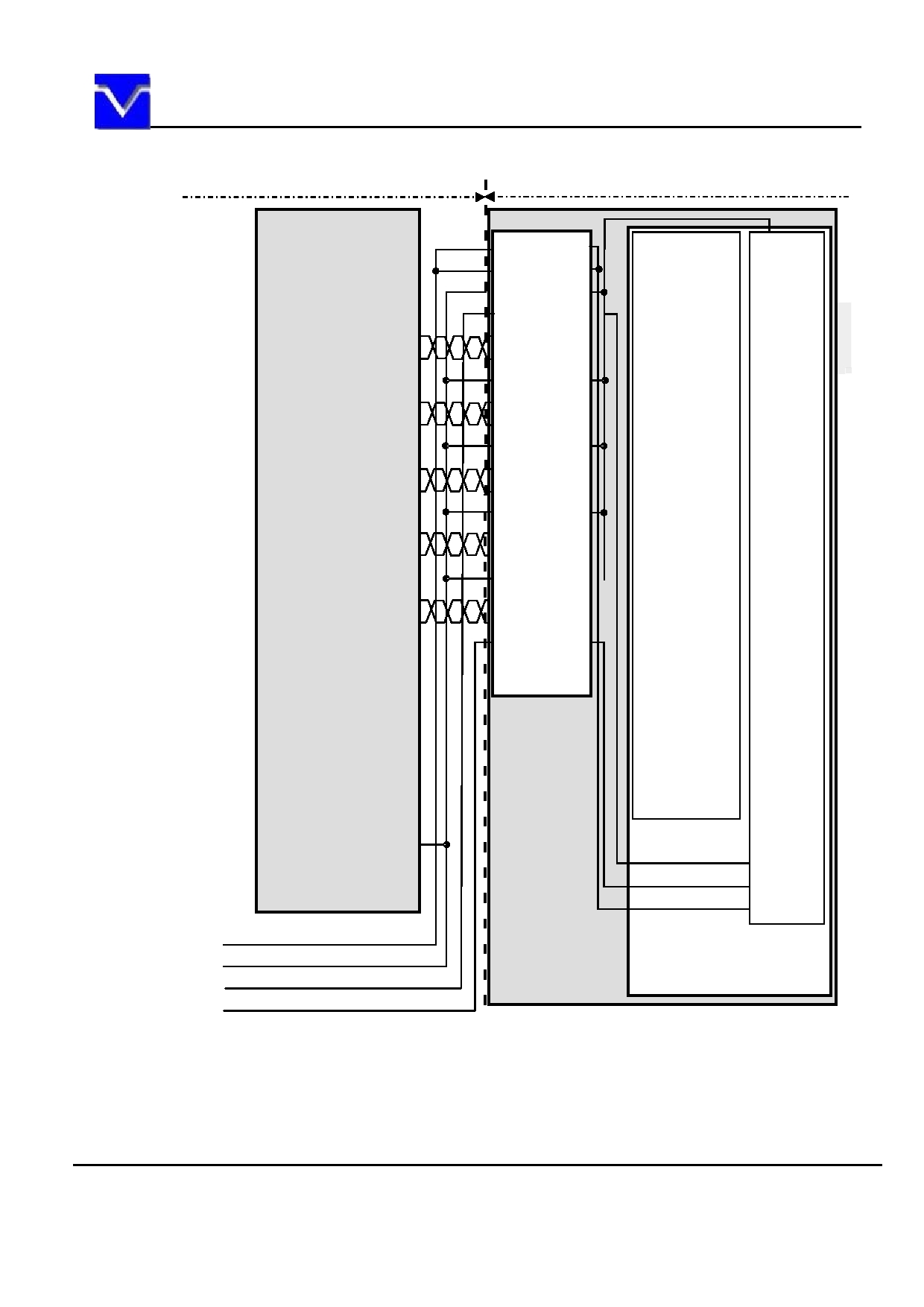
4.5.4 Connection between receiver and transmitter for LVDS
(1) Input data signal: 8-bit (FRC: High)
Host
LCD module (Product)
Note2
R0
TA0
Note3
R1
TA1
1
VCC
GND
R2
TA2
2
VCC
R3
TA3
3
GND
R4
TA4
4
FRC
R5
TA5
TA-
5
D0-
RA-
G0
TA6
TA+
6
D0+
RA+
7
GND
G1
TB0
TB-
8
D1-
RB-
G2
TB1
TB+
9
D1+
RB+
G3
TB2
10
GND
G4
TB3
TC-
11
D2-
RC-
G5
TB4
TC+
12
D2+
RC+
Signal
B0
TB5
13
GND
processor
B1
TB6
TCLK-
14
CLK-
RCLK-
TCLK+
15
CLK+
RCLK+
B2
TC0
16
GND
B3
TC1
TD-
17
D3-
RD-
B4
TC2
TD+
18
D3+
RD+
B5
TC3
19
DPS
Note4
TC4
20
N.C.
Note4
TC5
DE
TC6
Receiver for LVDS
CN1
R6
TD0
R7
TD1
G6
TD2
G7
TD3
B6
TD4
B7
TD5
GND
FRC
Note4
TD6
DPS
CLK
CLK IN
VCC
LVDS transmitter
Note1
THC63LVDM83C(5S) or equivalent
VCC
GND
FRC
LCD controller
DPS
LCD panel signal processing board
Note1: Recommended transmitter: THC63LVDM83C(5S) (THine Electronics Inc.) or equivalent.
Note2: LSB (Least Significant Bit) - R0, G0, B0 MSB (Most Significant Bit) - R7, G7, B7
Note3: Twist pair wires with 100 (Characteristic impedance) should be used between LCD panel
signal processing board and LVDS transmitter.
Note4: Input signals to TC4, TC5 and TD6 are not used inside the product, but do not keep them
open to avoid noise problem.
URL: www.topwaydisplay.com
Page 15 of 32
SHANGHAI AVIC OPTOELECTRONICS
Model No.TM121TDSG02
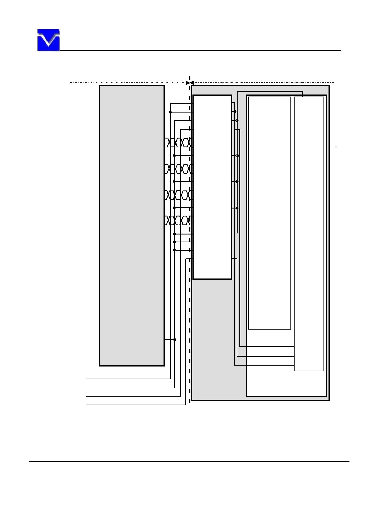
(2) Input data signal: 6-bit (FRC: Low or Open)
Host
LCD module (Product)
Note2
R0
TA0
Note3
R1
TA1
1
VCC
GND
R2
TA2
2
VCC
R3
TA3
3
GND
R4
TA4
4
FRC
R5
TA5
TA-
5
D0-
RA-
G0
TA6
TA+
6
D0+
RA+
7
GND
G1
TB0
TB-
8
D1-
RB-
G2
TB1
TB+
9
D1+
RB+
G3
TB2
10
GND
G4
TB3
TC-
11
D2-
RC-
G5
TB4
TC+
12
D2+
RC+
Signal
B0
TB5
13
GND
processor
B1
TB6
TCLK-
14
CLK-
RCLK-
TCLK+
15
CLK+
RCLK+
B2
TC0
16
GND
B3
TC1
TD-
17
GND
B4
TC2
TD+
18
GND
B5
TC3
19
DPS
Note4
TC4
20
N.C.
Note4
TC5
DE
TC6
Receiver for LVDS
CN1
Note4
TD0
Note4
TD1
Note4
TD2
Note4
TD3
Note4
TD4
Note4
TD5
GND
FRC
Note4
TD6
DPS
CLK
CLK IN
VCC
LVDS transmitter
Note1
THC63LVDM83C(5S) or equivalent
VCC
GND
FRC
LCD controller
DPS
LCD panel signal processing board
Note1: Recommended transmitter: THC63LVDM83C(5S) (THine Electronics Inc.) or equivalent.
Note2: LSB (Least Significant Bit) - R0, G0, B0 MSB (Most Significant Bit) - R5, G5, B5
Note3: Twist pair wires with 100 (Characteristic impedance) should be used between LCD panel
signal processing board and LVDS transmitter.
Note4: Input signals to TC4, TC5 and TD0-6 are not used inside the product, but do not keep them
open to avoid noise problem.
URL: www.topwaydisplay.com
Page 16 of 32
SHANGHAI AVIC OPTOELECTRONICS
Model No.TM121TDSG02
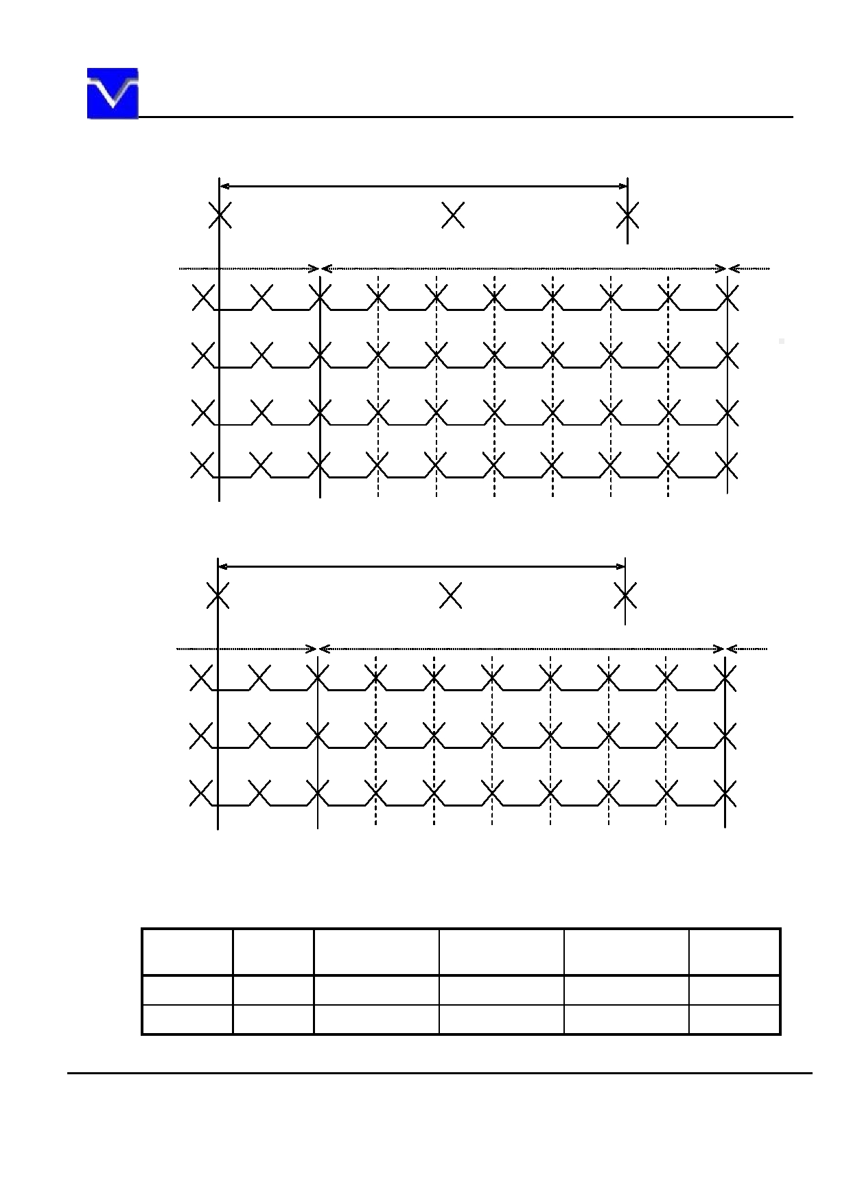
4.5.5 Input data mapping
(1) LVDS Input data signal: 8-bit
tc
CLK+/-
1CLK
D0+/-
G0
R5
R4
R3
R2
R1
R0
D1+/-
B1
B0
G5
G4
G3
G2
G1
D2+/-
DE
-
-
B5
B4
B3
B2
D3+/-
-
B7
B6
G7
G6
R7
R6
(2) LVDS Input data signal: 6-bit
tc
CLK+/-
1CLK
D0+/-
G0
R5
R4
R3
R2
R1
R0
D1+/-
B1
B0
G5
G4
G3
G2
G1
D2+/-
DE
-
-
B5
B4
B3
B2
4.6 DISPLAY COLORS AND INPUT DATA SIGNALS
4.6.1 Combinations of input data signals and FRC signal
This product can display 16,194,277 colors with 253 gray scales and 262,144 colors with 64 gray
scales by combination of input data signals and FRC signal. See the following table.
Input data
CN1-
Combination
FRC terminal
Display colors
Remarks
signals
Pin No.17 and 18
①
8-bit
D3+/-
High
16,194,277
Note1
②
6-bit
GND
Low or Open
262,144
Note2
Note1: See " 4.6.2 16,194,277 colors ".
Note2: See " 4.6.3 262,144 colors ".
URL: www.topwaydisplay.com
Page 17 of 32

SHANGHAI AVIC OPTOELECTRONICS
Model No.TM121TDSG02
4.6.2 16,194,277 colors
This product can display 16,194,277 colors with 253 gray scales by combination ① .
(See " 4.6.1 Combinations of input data signals and FRC signal ".)
Also the relation between display colors and input data signals is as follows.
Data signal (0: Low level, 1: High level)
Display colors
R7 R6 R5 R4 R3 R2 R1 R0
G7 G6 G5 G4 G3 G2 G1 G0
B7 B6 B5 B4 B3 B2 B1 B0
Black
0
0
0
0
0
0
0
0
0
0
0
0
0
0
0
0
0
0
0
0
0
0
0
0
Blue
0
0
0
0
0
0
0
0
0
0
0
0
0
0
0
0
1
1
1
1
1 1
1
1
Red
1
1
1
1
1
1
1
1
0
0
0
0
0
0
0
0
0
0
0
0
0
0
0
0
Magenta
1
1
1
1
1
1
1
1
0
0
0
0
0
0
0
0
1
1
1
1
1
1
1
1
Green
0
0
0
0
0
0
0
0
1
1
1
1
1
1
1
1
0
0
0
0
0
0
0
0
Cyan
0
0
0
0
0
0
0
0
1
1
1
1
1
1
1
1
1
1
1
1
1
1
1
1
Yellow
1
1
1
1
1
1
1
1
1
1
1
1
1
1
1
1
0
0
0
0
0
0
0
0
White
1
1
1
1
1
1
1
1
1
1
1
1
1
1
1
1
1
1
1
1
1
1
1
1
Black
0
0
0
0
0
0
0
0
0
0
0
0
0
0
0
0
0
0
0
0
0
0
0
0
0
0
0
0
0
0
0
1
0
0
0
0
0
0
0
0
0
0
0
0
0
0
0
0
dark
0
0
0
0
0
0
1
0
0
0
0
0
0
0
0
0
0
0
0
0
0
0
0
0
:
:
:
:
:
:
bright
1
1
1
1
1
1
0
1
0
0
0
0
0
0
0
0
0
0
0
0
0
0
0
0
1
1
1
1
1
1
1
0
0
0
0
0
0
0
0
0
0
0
0
0
0
0
0
0
Red
1
1
1
1
1
1
1
1
0
0
0
0
0
0
0
0
0
0
0
0
0
0
0
0
Black
0
0
0
0
0
0
0
0
0
0
0
0
0
0
0
0
0
0
0
0
0
0
0
0
0
0
0
0
0
0
0
0
0
0
0
0
0
0
0
1
0
0
0
0
0
0
0
0
dark
0
0
0
0
0
0
0
0
0
0
0
0
0
0
1
0
0
0
0
0
0
0
0
0
:
:
:
:
:
:
bright
0
0
0
0
0
0
0
0
1
1
1
1
1
1
0
1
0
0
0
0
0
0
0
0
0
0
0
0
0
0
0
0
1
1
1
1
1
1
1
0
0
0
0
0
0
0
0
0
Green
0
0
0
0
0
0
0
0
1
1
1
1
1
1
1
1
0
0
0
0
0
0
0
0
Black
0
0
0
0
0
0
0
0
0
0
0
0
0
0
0
0
0
0
0
0
0
0
0
0
0
0
0
0
0
0
0
0
0
0
0
0
0
0
0
0
0
0
0
0
0
0
0
1
dark
0
0
0
0
0
0
0
0
0
0
0
0
0
0
0
0
0
0
0
0
0
0
1
0
:
:
:
:
:
:
bright
0
0
0
0
0
0
0
0
0
0
0
0
0
0
0
0
1
1
1
1
1
1
0
1
0
0
0
0
0
0
0
0
0
0
0
0
0
0
0
0
1
1
1
1
1
1
1
0
Blue
0
0
0
0
0
0
0
0
0
0
0
0
0
0
0
0
1
1
1
1
1
1
1
1
URL: www.topwaydisplay.com
Page 18 of 32

SHANGHAI AVIC OPTOELECTRONICS
Model No.TM121TDSG02
4.6.3 262,144 colors
This product can display 262,144 colors with 64 gray scales by combination ② .
(See " 4.6.1 Combinations of input data signals and FRC signal ".)
Also the relation between display colors and input data signals is as follows.
Data signal (0: Low level, 1: High level)
Display colors
R 5 R 4 R 3 R 2 R 1 R 0 G5 G4 G3 G2 G1 G0
B 5 B 4 B 3 B 2 B 1 B 0
Black
0
0
0
0
0
0
0
0
0
0
0
0
0
0
0
0
0
0
Blue
0
0
0
0
0
0
0
0
0
0
0
0
1
1
1
1
1
1
Red
1
1
1
1
1
1
0
0
0
0
0
0
0
0
0
0
0
0
Magenta
1
1
1
1
1
1
0
0
0
0
0
0
1
1
1
1
1
1
Green
0
0
0
0
0
0
1
1
1
1
1
1
0
0
0
0
0
0
Cyan
0
0
0
0
0
0
1
1
1
1
1
1
1
1
1
1
1
1
Yellow
1
1
1
1
1
1
1
1
1
1
1
1
0
0
0
0
0
0
White
1
1
1
1
1
1
1
1
1
1
1
1
1
1
1
1
1
1
Black
0
0
0
0
0
0
0
0
0
0
0
0
0
0
0
0
0
0
0
0
0
0
0
1
0
0
0
0
0
0
0
0
0
0
0
0
dark
0
0
0
0
1
0
0
0
0
0
0
0
0
0
0
0
0
0
:
:
:
:
:
:
bright
1
1
1
1
0
1
0
0
0
0
0
0
0
0
0
0
0
0
1
1
1
1
1
0
0
0
0
0
0
0
0
0
0
0
0
0
Red
1
1
1
1
1
1
0
0
0
0
0
0
0
0
0
0
0
0
Black
0
0
0
0
0
0
0
0
0
0
0
0
0
0
0
0
0
0
0
0
0
0
0
0
0
0
0
0
0
1
0
0
0
0
0
0
dark
0
0
0
0
0
0
0
0
0
0
1
0
0
0
0
0
0
0
:
:
:
:
:
:
bright
0
0
0
0
0
0
1
1
1
1
0
1
0
0
0
0
0
0
0
0
0
0
0
0
1
1
1
1
1
0
0
0
0
0
0
0
Green
0
0
0
0
0
0
1
1
1
1
1
1
0
0
0
0
0
0
Black
0
0
0
0
0
0
0
0
0
0
0
0
0
0
0
0
0
0
0
0
0
0
0
0
0
0
0
0
0
0
0
0
0
0
0
1
dark
0
0
0
0
0
0
0
0
0
0
0
0
0
0
0
0
1
0
:
:
:
:
:
:
bright
0
0
0
0
0
0
0
0
0
0
0
0
1
1
1
1
0
1
0
0
0
0
0
0
0
0
0
0
0
0
1
1
1
1
1
0
Blue
0
0
0
0
0
0
0
0
0
0
0
0
1
1
1
1
1
1
URL: www.topwaydisplay.com
Page 19 of 32
SHANGHAI AVIC OPTOELECTRONICS
Model No.TM121TDSG02
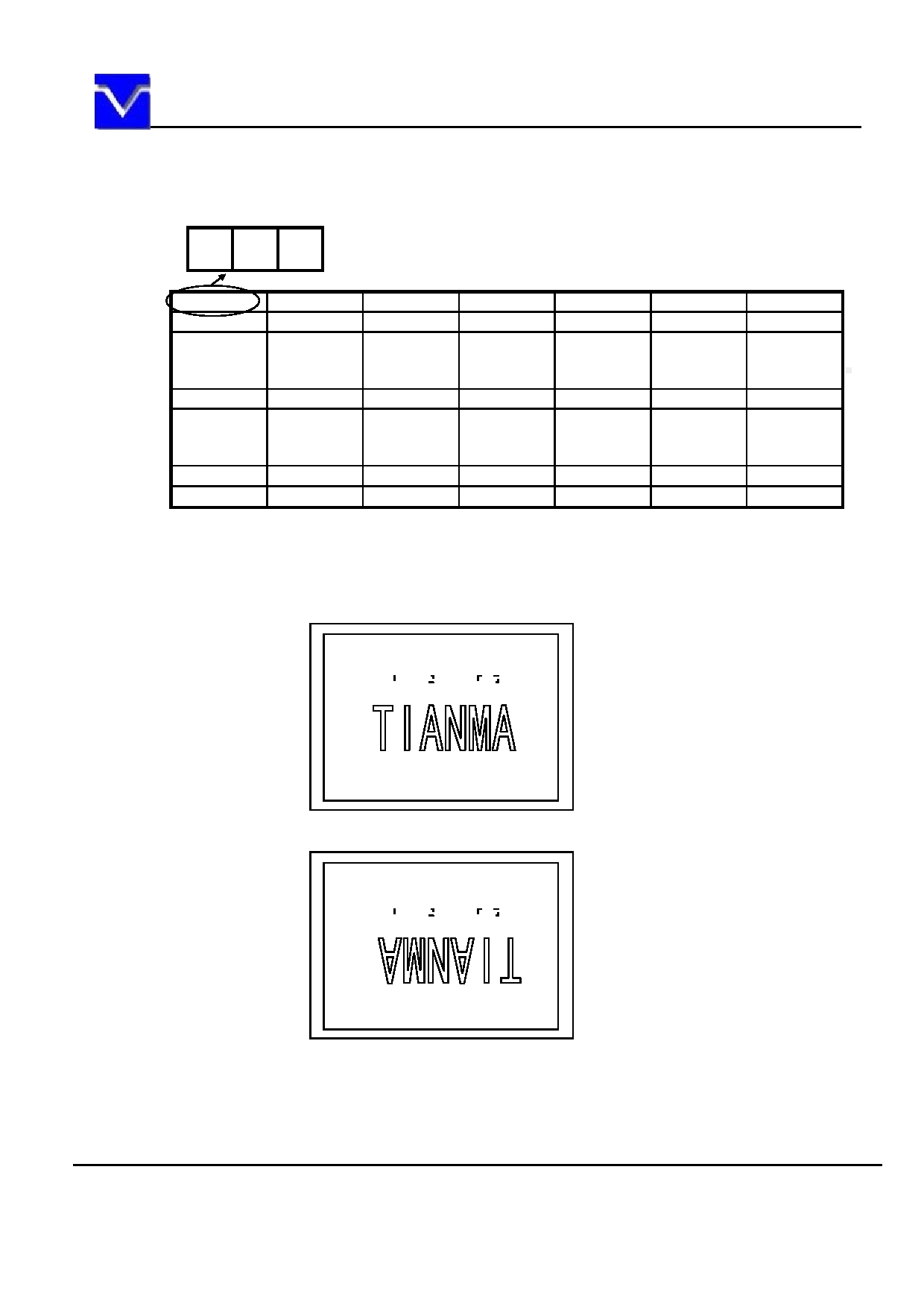
4.7 DISPLAY POSITIONS
The following table is the coordinates per pixel (See " 4.8 SCANNING DIRECTIONS ".).
C (0, 0)
B
G
R
C( 0, 0)
C( 1, 0)
∙ ∙ ∙
C( X, 0)
∙ ∙ ∙
C(1022, 0)
C(1023, 0)
C( 0, 1)
C( 1, 1)
∙ ∙ ∙
C( X, 1)
∙ ∙ ∙
C(1022, 1)
C(1023, 1)
∙
∙
∙
∙
∙
∙
∙
∙
∙
∙ ∙ ∙
∙
∙ ∙ ∙
∙
∙ ∙ ∙
∙
∙
∙
∙
∙
∙
∙
C( 0, Y)
C( 1, Y)
∙ ∙ ∙
C( X, Y)
∙ ∙ ∙
C(1022, Y)
C(1023, Y)
∙
∙
∙
∙
∙
∙
∙
∙
∙
∙ ∙ ∙
∙
∙ ∙ ∙
∙
∙
∙
∙
∙
∙
∙
∙
∙
C( 0, 766)
C( 1, 766)
∙ ∙ ∙
C( X, 766)
∙ ∙ ∙
C(1022, 766)
C(1023, 766)
C( 0, 767)
C( 1, 767)
∙ ∙ ∙
C( X, 767)
∙ ∙ ∙
C(1022, 767)
C(1023, 767)
4.8 SCANNING DIRECTIONS
The following figures are seen from a front view.
C (0, 0)
C (1023, 0)
D (0, 0)
D (1023, 0)
CN1
CN2
Note1
C (0, 767)
C (1023, 767)
D (0, 767)
D (1023, 767)
Figure1. Normal scan (DPS: Low or Open)
C (0, 0)
C (1023, 0)
D (1023, 767)
D (0, 767)
CN1
CN2
Note1
C (0, 767)
C (1023, 767)
D (1023, 0)
D (0, 0)
Figure2. Reverse scan (DPS: High)
Note1: Meaning of C (X, Y) and D (X, Y)
C (X, Y): The coordinates of the display position (See " 4.7 DISPLAY POSITIONS ".)
D (X, Y): The data number of input signal for LCD panel signal processing board
URL: www.topwaydisplay.com
Page 20 of 32
SHANGHAI AVIC OPTOELECTRONICS
Model No.TM121TDSG02
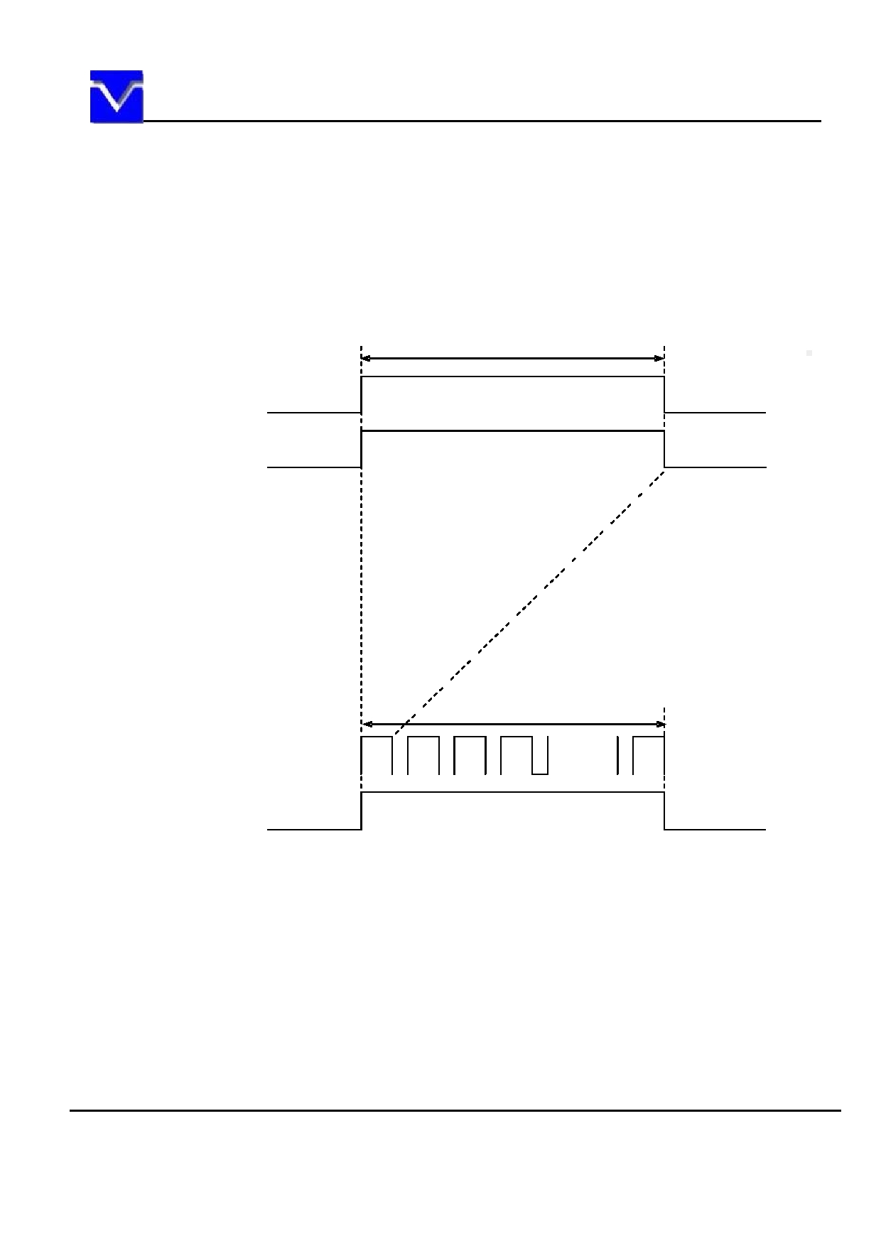
4.9 INPUT SIGNAL TIMINGS
4.9.1 Outline of input signal timings
Horizontal signal
Note1
Horizontal display period (thd)
DE (Data enable)
Display period
Vertical signal
Note1
Vertical display period (tvd)
DE (Data enable)
1
2
3
4
768
Note2
Display period
Note1: This diagram indicates virtual signal for set up to timing.
Note2: See " 4.9.3 Input signal timing chart " for the pulse number.
URL: www.topwaydisplay.com
Page 21 of 32
SHANGHAI AVIC OPTOELECTRONICS
Model No.TM121TDSG02
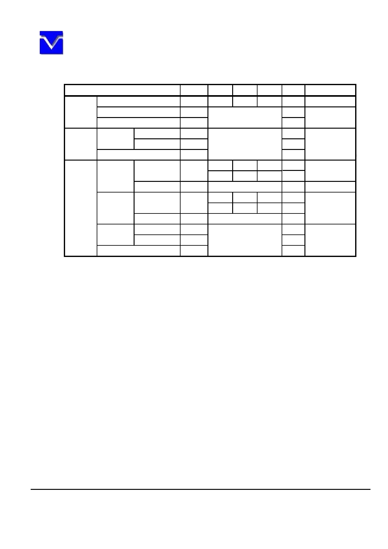
4.9.2 Timing characteristics
(Note1, Note2, Note3)
Parameter
Symbol
min.
typ.
max.
Unit
Remarks
Frequency
1/tc
52.0
65.0
71.0
MHz
15.385ns (typ.)
CLK
Duty ratio
-
-
-
-
Rise time, Fall time
-
ns
Setup time
-
ns
CLK-DATA
DATA
Hold time
-
-
ns
-
Rise time, Fall time
-
ns
16.542
20.676
26.88
s
Cycle
th
48.363kHz (typ.)
Horizontal
1,114
1,344
1,400
CLK
Display period
thd
1024
CLK
-
13.34
16.666
20.0
ms
Vertical
Cycle
tv
DE
780
806
845
H
60.0Hz (typ.)
(One frame)
Display period
tvd
768
H
Setup time
-
ns
CLK-DE
Hold time
-
-
ns
-
Rise time, Fall time
-
ns
Note1: Definition of parameters is as follows.
tc= 1CLK, th= 1H
Note2: See the data sheet of LVDS transmitter.
Note3: Vertical cycle (tv) should be specified in integral multiple of Horizontal cycle (th).
URL: www.topwaydisplay.com
Page 22 of 32
SHANGHAI AVIC OPTOELECTRONICS
Model No.TM121TDSG02
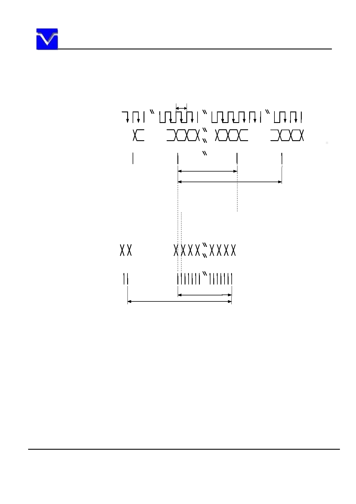
4.9.3 Input signal timing chart
Horizontal timing
tc
CLK
DATA
(R0-R5)
(R0-R7)
(G0-G5) or (G0-G7)
INVALID
1
2
1023 1024
INVALID
(B0-B5)
(B0-B7)
DE
thd
th
Vertical timing
DATA
(R0-R5)
(R0-R7)
(G0-G5) or (G0-G7)
INVALID
INVALID
(B0-B5)
(B0-B7)
1 2
767 768
DE
tvd
tv
URL: www.topwaydisplay.com
Page 23 of 32
SHANGHAI AVIC OPTOELECTRONICS
Model No.TM121TDSG02
4.10 OPTICS
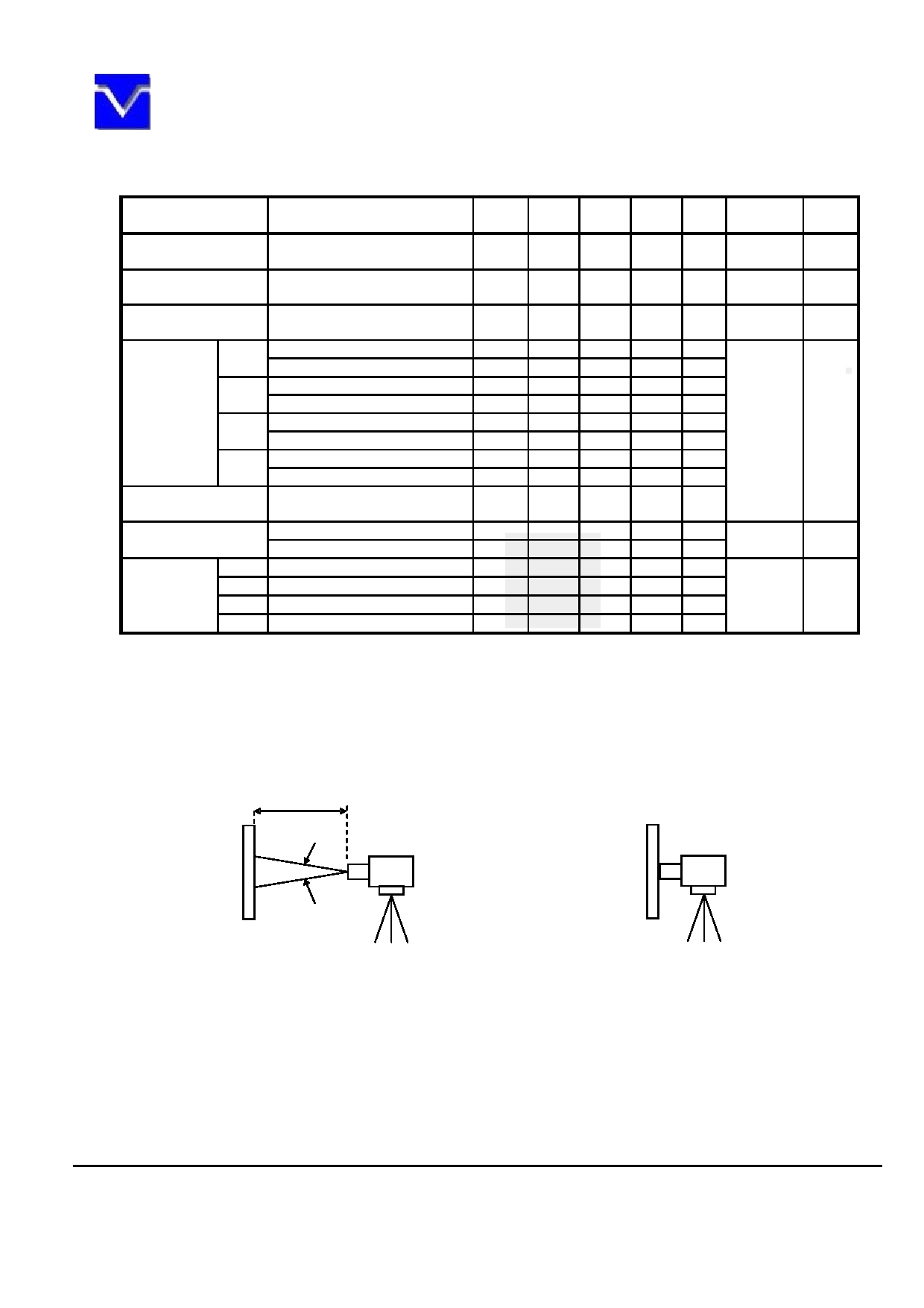
4.10.1 Optical characteristics
(Note1, Note2)
Measuring
Parameter
Condition
Symbol
min.
typ.
max.
Unit
Remarks
instrument
White at center
Luminance
R= 0 , L = 0 , U = 0 , D = 0
L
300
450
-
cd/m 2
SR-UL1R
-
White/Black at center
Contrast ratio
R= 0 , L = 0 , U = 0 , D = 0
CR
500
700
-
-
SR-UL1R
Note3
Luminance uniformity
White
R= 0 , L = 0 , U = 0 , D = 0
LU
-
1.25
1.33
-
SR-UL1R
Note4
x coordinate
Wx
0.263
0.313
0.363
-
White
y coordinate
Wy
0.279
0.329
0.379
-
x coordinate
Rx
0.529
0.579
0.629
-
Red
y coordinate
Ry
0.290
0.340
0.390
-
Chromaticity
x coordinate
Gx
0.277
0.327
0.377
-
Green
SR-UL1R
Note5
y coordinate
Gy
0.553
0.603
0.653
-
x coordinate
Bx
0.105
0.155
0.205
-
Blue
y coordinate
By
0.038
0.088
0.138
-
R= 0 , L = 0 , U = 0 , D = 0
Color gamut
C
48
55
-
%
at center, against NTSC color space
White to Black
Ton
-
3
5
ms
TRD
Note6
Response time
Black to White
Toff
-
5
8
ms
-100
Note7
Right
U= 0 , D = 0 , C R 10
R
70
80
-
Left
U= 0 , D = 0 , C R 10
L
70
80
-
EZ
Viewing angle
Note8
Up
R= 0 , L = 0 , C R 10
U
70
80
-
Contrast
Down
R= 0 , L = 0 , C R 10
D
70
80
-
Note1: These are initial characteristics.
Note2: Measurement conditions are as follows.
Ta= 25 C, VCC= 3.3V, VDD= 12.0V, PWM duty ratio: 100%,
Display mode: XGA, Horizontal cycle= 1/48.363kHz, Vertical cycle= 1/60.0Hz,
DPS= Low or Open: Normal scan, FRC=Low
Optical characteristics are measured at luminance saturation 20minutes after the product
works in the dark room. Also measurement methods are as follows.
50cm
Photodetector
Photodetector (EZ Contrast)
1
LCD module
LCD module
(Product)
(Product)
Note3: See " 4.10.2 Definition of contrast ratio ".
Note4: See " 4.10.3 Definition of luminance uniformity ".
Note5: These coordinates are found on CIE 1931 chromaticity diagram.
Note6: Product surface temperature: TopF= 29 C
Note7: See " 4.10.4 Definition of response times ".
Note8: See " 4.10.5 Definition of viewing angles ".
URL: www.topwaydisplay.com
Page 24 of 32
SHANGHAI AVIC OPTOELECTRONICS
Model No.TM121TDSG02
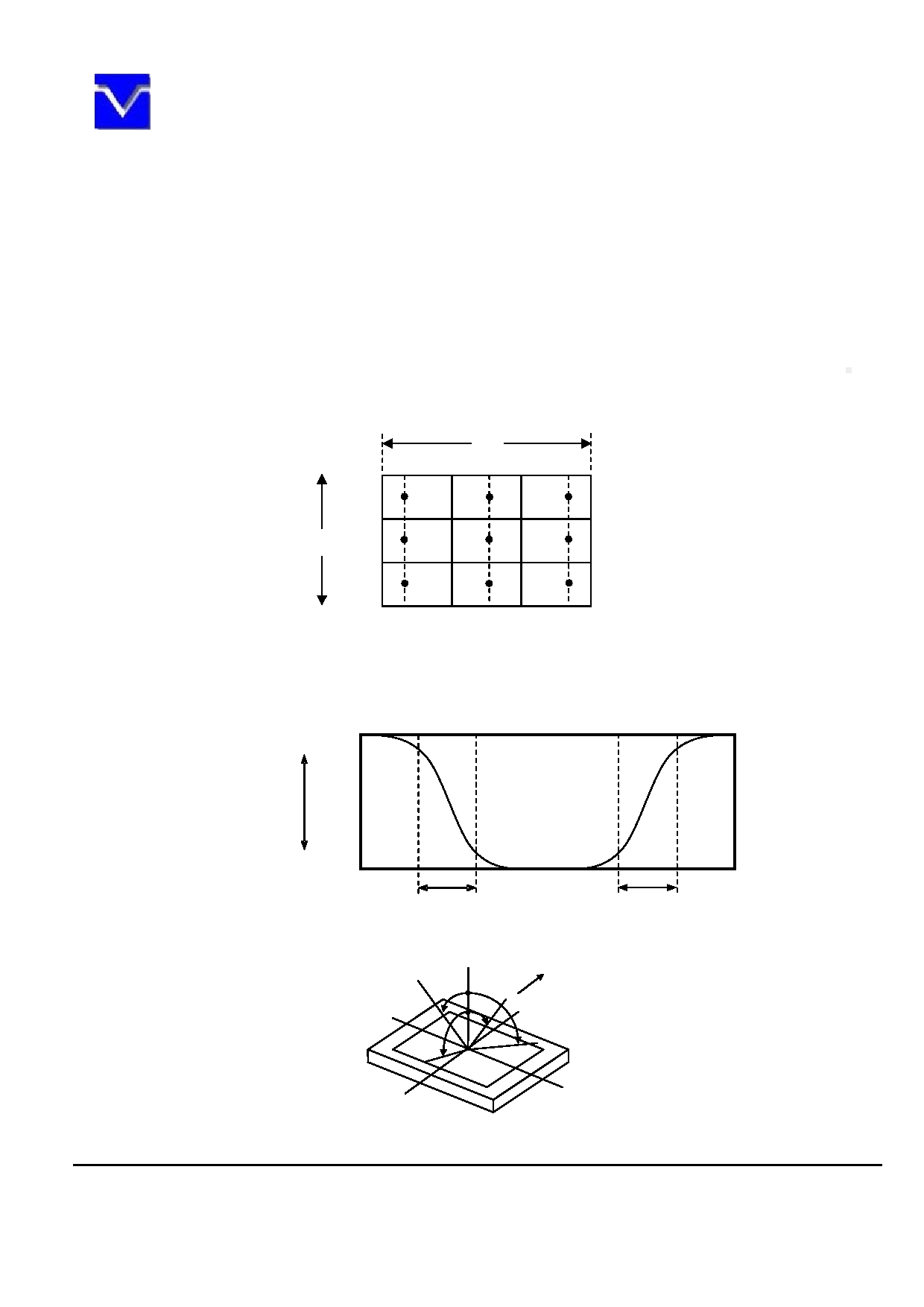
4.10.2 Definition of contrast ratio
The contrast ratio is calculated by using the following formula.
Luminance of white screen
Contrast ratio (CR) =
Luminance of black screen
4.10.3 Definition of luminance uniformity
The luminance uniformity is calculated by using following formula.
Maximum luminance from ① to ⑨
Luminance uniformity (LU) =
Minimum luminance from ① to ⑨
The luminance is measured at near the 9 points shown below.
H
H/6
H/2
H/6
①
②
③
V/6
④
⑤
⑥
V V/2
⑦
⑧
⑨
V/6
4.10.4 Definition of response times
Response time is measured at the time when the luminance changes from " white " to " black ",
or " black " to " white " on the same screen point, by photo-detector. Ton is the time when the
luminance changes from 90% down to 10%. Also Toff is the time when the luminance changes
from 10% up to 90% (See the following diagram.).
100%
White
90%
Luminance
Black
10%
0%
Ton
Toff
4.10.5 Definition of viewing angles
Normal axis (Perpendicular)
L
12 o’clock
U
Left
Upper
R
D
CN1
CN2
Lower
Right
URL: www.topwaydisplay.com
Page 25 of 32

SHANGHAI AVIC OPTOELECTRONICS
Model No.TM121TDSG02
5. ESTIMATED LUMINANCE LIFETIME
The luminance lifetime is the time from initial luminance to half-luminance.
This lifetime is the estimated value, and is not guarantee value.
Estimated luminance lifetime
Condition
(Life time expectancy)
Unit
Note1
25 C (Ambient temperature of the product)
LED lifetime
Continuous operation, PWM duty ratio: 100%
50,000
H
Note1: Optical performance should be evaluated at Ta=25 ℃ only If LED is driven by high current,
high ambient temperature & humidity condition. The life time of LED will be reduced.
Operating life means brightness goes down to 50% initial brightness. Typical operating life
time is estimated data.
URL: www.topwaydisplay.com
Page 26 of 32

SHANGHAI AVIC OPTOELECTRONICS
Model No.TM121TDSG02
6. RELIABILITY TESTS
No
Test Item
Condition
Remarks
1
High Temperature
IEC60068-2-1:2007
Operation
Ts = +70 ℃ , 240 hours (Note1)
GB2423.2-2008
2
Low Temperature
IEC60068-2-1:2007
Operation
Ta = -20 ℃ , 240 hours (Note1)
GB2423.1-2008
3
High Temperature
IEC60068-2-1:2007
Storage
Ta = +80 ℃ , 240 hours
GB2423.2-2008
4
Low Temperature
IEC60068-2-1:2007
Storage
Ta = -30 ℃ , 240 hours
GB2423.1-2008
Storage at High
5
Temperature and
Ta = +50 ℃ , 80% RH max, 240hours
IEC60068-2-78 :2001
Humidity
GB/T2423.3—2006
Start with cold temperature,
6
Thermal Shock
-20 ℃ 30 min ~ +60 ℃ 30 min,
End with high temperature,
(non-operation)
Change time:5min, 20 Cycle
IEC60068-2-14:1984,
GB2423.22-2002
C=150pF, R=330Ω,
Air: ±15Kv, 9points,25times/point;
7
ESD(Operation)
Contact: ±8Kv, 9points,25times/point
IEC61000-4-2:2001
(Environment: 15 ℃ ~35 ℃ , 30%~60%.
GB/T17626.2-2006
86Kpa~106Kpa)
8
Package Drop Test
Height: 60cm,
IEC60068-2-32:1990
1corner, 3edges, 6surfaces
GB/T2423.8—1995
Frequency range:5~100Hz,11.76m/s ²
9
Vibration
1minute/cycle
IEC600682-6:1982
(Non-operation)
X,Y,Z directions
GB2423.10-1995
50times each directions
10
Shock
30G,11ms, ± X,Y,Z directions,3times
IEC60068-2-27:1987
(Non-operation)
For each direction
GB/T2423.5 — 1995
Note1: Ts is the temperature of panel’s surface.
Note2: Ta is the ambient temperature of sample.
Note3: Before cosmetic and function test, the product must have enough recovery time, at least 2 hours at room
temperature.
Note 4: In the standard condition, there shall be no practical problem that may affect the display function. After
the reliability test, the product only guarantees operation, but don’t guarantee all of the cosmetic specification.
URL: www.topwaydisplay.com
Page 27 of 32

SHANGHAI AVIC OPTOELECTRONICS
Model No.TM121TDSG02
7. MARKINGS
The various markings are attached to this product. See "10. OUTLINE DRAWINGS" for
attachment positions.
7.1 NAMEPLATE LABEL
TBD
7.2 BARCODE LABEL
TBD
URL: www.topwaydisplay.com
Page 28 of 32

SHANGHAI AVIC OPTOELECTRONICS
Model No.TM121TDSG02
8. PACKING, TRANSPORTATION AND DELIVERY
AVIC will pack products to deliver to customer in accordance with AVIC's packing specifications,
and will deliver products to customer in such a condition that products will not suffer from damage
during transportation. The delivery conditions are as follows.
8.1 INNER PACKING BOX
10 products are packed as the maximum in an inner packing box (See " 8.6 OUTLINE FIGURE
FOR PACKING "). The type name and quantity are shown on outside of the inner packing box,
either labeling or printing. In case the inner packing box with products is dropped from a height of
60cm or more, there is a risk of damage to products.
8.2 OUTER PACKING BOX
The inner box with products is packed in an outer packing box (See " 8.6 OUTLINE FIGURE
FOR PACKING "). The type name and quantity are shown on outside of the outer packing box,
either labeling or printing. In case the outer packing box with products is dropped from a height of
60cm or more, there is a risk of damage to products.
8.3 INSPECTION RECORD SHEET
Inspection record sheets are included in an inner packing box with products. It is summarized to a
number of products for pass/fail assessment.
8.4 TRANSPORTATION
The product is transported by vehicle and aircraft.
8.5 SIZE AND WEIGHT FOR PACKING BOXES
TBD
8.6 OUTLINE FIGURE FOR PACKING
TBD
URL: www.topwaydisplay.com
Page 29 of 32

SHANGHAI AVIC OPTOELECTRONICS
Model No.TM121TDSG02
9. PRECAUTIONS
9.1 MEANING OF CAUTION SIGNS
The following caution signs have very important meaning. Be sure to read "9.2 CAUTIONS"
and "9.3 ATTENTIONS"!
!
This sign has the meaning that a customer will be injured or the product will sustain
damage if the customer practices wrong operations.
This sign has the meaning that a customer will be injured if the customer practices
wrong operations.
9.2 CAUTIONS
Do not shock and press the LCD panel and the backlight! There is a danger of breaking,
because they are made of glass. (Shock: Equal to or no greater than 539m/s and equal to
2
or no greater than 11ms, Pressure: Equal to or no greater than 19.6 N ( 16mm jig))
9.3 ATTENTIONS
!
9.3.1 Handling of the product
① Take hold of both ends without touching the circuit board when the product (LCD module) is
picked up from inner packing box to avoid broken down or misadjustment, because of stress to
mounting parts on the circuit board.
② When the product is put on the table temporarily, display surface must be placed downward.
③ When handling the product, take the measures of electrostatic discharge with such as earth band,
ionic shower and so on, because the product may be damaged by electrostatic.
④ The torque for product mounting screws must never exceed 0.392N m. Higher torque might
result in distortion of the bezel.
⑤ The product must be installed using mounting holes without undue stress such as bends or twist
(See outline drawings). And do not add undue stress to any portion (such as bezel flat area).
Bends or twist described above and undue stress to any portion may cause display mura.
⑥ Do not press or rub on the sensitive product surface. When cleaning the product surface, wipe it a
soft dry cloth.
⑦ Do not push or pull the interface connectors while the product is working.
⑧ When handling the product, use of an original protection sheet on the product surface (polarizer)
is recommended for protection of product surface. Adhesive type protection sheet may change
color or characteristics of the polarizer.
⑨ Usually liquid crystals don't leak through the breakage of glasses because of the surface tension
of thin layer and the construction of LCD panel. But, if you contact with liquid crystal by any
chance, please wash it away with soap and water.
URL: www.topwaydisplay.com
Page 30 of 32

SHANGHAI AVIC OPTOELECTRONICS
Model No.TM121TDSG02
9.3.2 Environment
① Do not operate or store in high temperature, high humidity, dewdrop atmosphere or corrosive
gases. Keep the product in packing box with antistatic pouch in room temperature to avoid dusts
and sunlight, when storing the product.
② In order to prevent dew condensation occurred by temperature difference, the product packing
box must be opened after enough time being left under the environment of an unpacking room.
Evaluate the storage time sufficiently because dew condensation is affected by the environmental
temperature and humidity. (Recommended leaving time: 6 hours or more with the original
packing state after a customer receives the package)
③ Do not operate in high magnetic field. If not, circuit boards may be broken.
④ This product is not designed as radiation hardened.
9.3.3 Characteristics
The following items are neither defects nor failures.
① Characteristics of the LCD (such as response time, luminance, color uniformity and so on) may
be changed depending on ambient temperature. If the product is stored under condition of low
temperature for a long time, it may cause display mura. In this case, the product should be
operated after enough time being left under condition of operating temperature.
② Display mura, flickering, vertical streams or tiny spots may be observed depending on display
patterns.
③ Do not display the fixed pattern for a long time because it may cause image sticking. Use a
screen saver, if the fixed pattern is displayed on the screen.
④ The display color may be changed depending on viewing angle because of the use of condenser
sheet in the backlight.
⑤ Optical characteristics may be changed depending on input signal timings.
9.3.4 Others
① All GND, VCC and VDD terminals should be used without any non-connected lines.
② Do not disassemble a product or adjust variable resistors.
③ See "REPLACEMENT MANUAL FOR LAMP HOLDER SET", when replacing lamp holder
set.
④ Pack the product with the original shipping package, in order to avoid any damages during
transportation, when returning the product to AVIC.
URL: www.topwaydisplay.com
Page 31 of 32
SHANGHAI AVIC OPTOELECTRONICS
Model No.TM121TDSG02
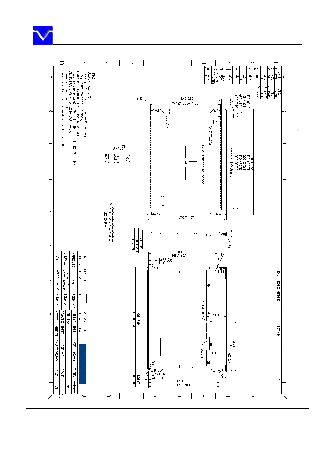
10. OUTLINE DRAWINGS
URL: www.topwaydisplay.com
Page 32 of 32
SHANGHAI AVIC OPTOELECTRONICS
Model No.TM121TDSG02
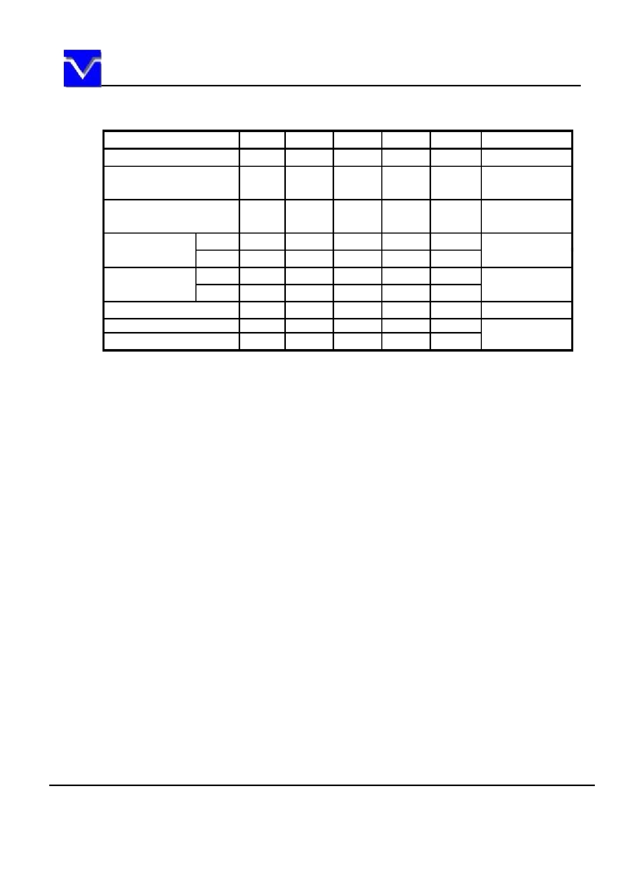
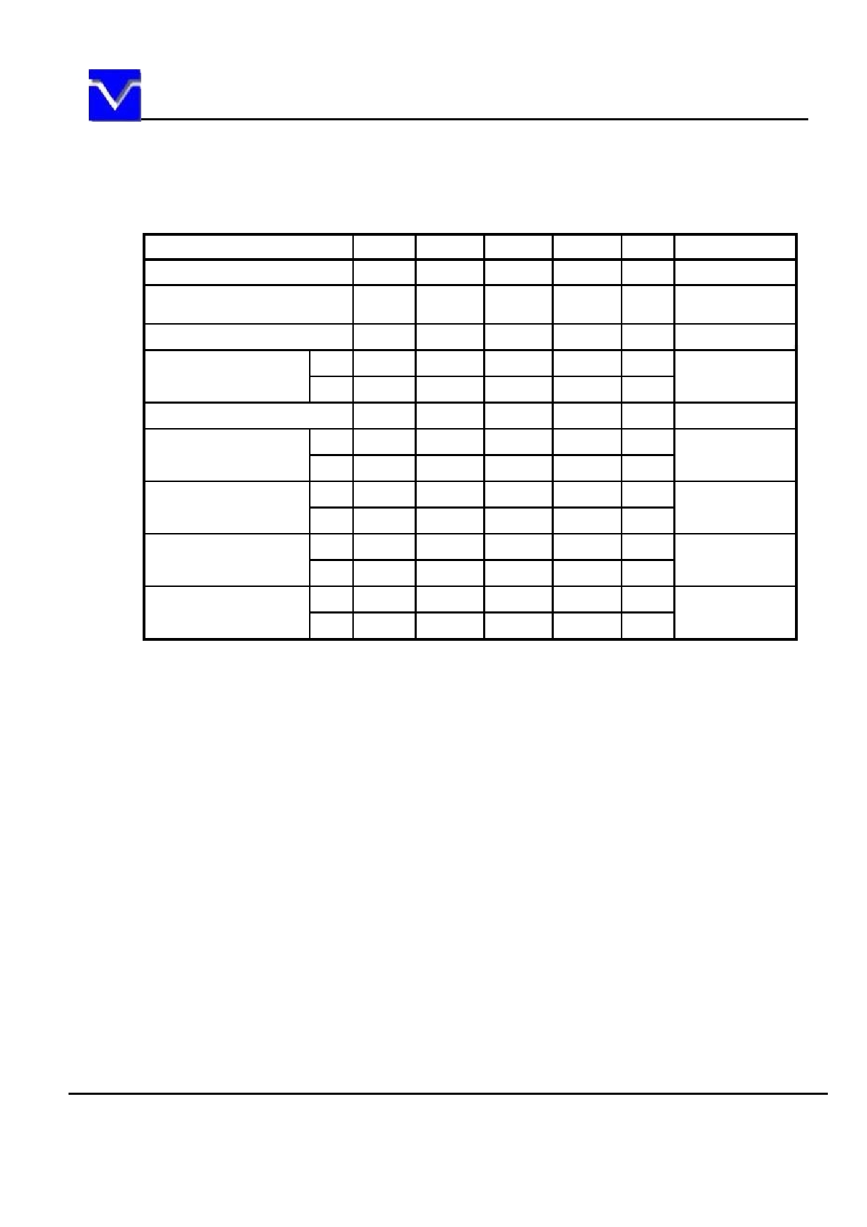
4.3 ELECTRICAL CHARACTERISTICS
4.3.1 LCD panel signal processing board
(Ta= 25 C)
Parameter
Symbol
min.
typ.
max.
Unit
Remarks
Power supply voltage
VCC
3.0
3.3
3.6
V
-
340
740
Power supply current
ICC
-
Note1
Note2
mA
at VCC= 3.3V
Permissible ripple voltage
VRP
-
-
300
mVp-p
for VCC
Differential input
High
VTH
-
-
+100
mV
at VCM= 1.25V
threshold voltage
Low
VTL
-100
-
-
mV
Note3
Terminating resistance
RT
-
100
-
-
Input voltage for DPS
High
VFH1
0.7VCC
-
VCC
V
-
signal
Low
VFL1
0
-
0.3VCC
V
Input voltage for FRC
High
VFH2
0.7VCC
-
VCC
V
-
signal
Low
VFL2
0
-
0.3VCC
V
Input current for DPS
High
IFH1
-
-
500
A
-
signal
Low
IFL1
-500
-
-
A
Input current for FRC
High
IFH2
-
-
300
A
-
signal
Low
IFL2
-300
-
-
A
Note1: Checkered flag pattern [by EIAJ ED-2522]
Note2: Pattern for maximum current
Note3: Common mode voltage for LVDS receiver
URL: www.topwaydisplay.com
Page 8 of 32