Designing LCD Backlight Driving Circuits: A Comprehensive Guide for Engineers
I. Introduction
Liquid Crystal Display (LCD) is a cornerstone of modern electronics, found in everything from smartphones to industrial equipment. While the LCD panel itself is responsible for displaying images, it's the backlight that truly brings them to life, illuminating the pixels and enabling visibility. Designing an efficient and reliable backlight driving circuit is crucial for optimal display performance, power consumption, and longevity. This blog post will delve into the intricacies of LCD backlight driving circuit design, covering common topologies, dimming techniques, and essential design considerations. We'll also use a real-world example, the LMT101DNLFWD-NND LCD module, to illustrate practical application.
II. Fundamentals of LCD Backlighting
The Evolution from CCFL to LED Backlights
Historically, cold cathode fluorescent lamps (CCFLs) were the dominant light source for LCD backlights. However, the industry has transitioned almost entirely to light-emitting diodes (LEDs) due to significant technological advantages. CCFLs operate at high voltages, contain a small amount of mercury, and can exhibit noticeable flickering, particularly at lower brightness settings. The rigid glass tubes of CCFLs also limit design flexibility, making them unsuitable for thin or flexible displays.
In contrast, LEDs offer superior energy efficiency, a longer operational lifespan, and a wider color gamut. The absence of mercury makes them a more environmentally friendly option. The compact size and solid-state nature of LEDs also provide greater design flexibility, enabling thinner and more robust display modules. This shift from high-voltage, AC-driven CCFLs to low-voltage, DC-driven LEDs has redefined the power management challenges for backlight units, shifting the focus to highly efficient, compact, and integrated DC-DC converters
The Imperative of Constant Current Driving
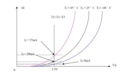
A fundamental principle of LED operation is that luminous intensity, or brightness, is directly proportional to the forward current flowing through the device. Unlike incandescent bulbs, an LED's forward voltage (Vf) is not fixed; it varies with temperature and can differ between manufacturing batches. Consequently, simply applying a constant voltage across an LED can result in significant current and brightness fluctuations if the voltage supply or ambient temperature changes. A simple resistive current limiter, while inexpensive, is highly inefficient as it dissipates excess energy as heat, making it unsuitable for high-power applications.
To ensure consistent brightness and long-term reliability, an LED backlight must be driven by a constant current source. Modern LED drivers are sophisticated integrated circuits that utilize closed-loop feedback to precisely regulate the output current, regardless of fluctuations in the input voltage or the LED's forward voltage. The presence of an integrated constant-current driver within the LMT101DNLFWD-NND module ensures that the backlight's performance is optimized, and the user is insulated from the complexities of designing this intricate power circuit.
III. Common Backlight Driving Topologies
While linear regulators are simple and have low part counts, their low efficiency makes them impractical for high-power LED backlights, as they dissipate a large amount of power as heat. The preferred solution for modern backlight applications is a switching regulator, which converts DC input power to a regulated DC output with much higher efficiency, typically in the range of 80% to 95%. The choice of switching topology depends on the relationship between the input voltage (Vin) and the required LED string voltage (Vout).
Boost Converters (Step-Up)
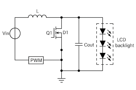
Boost converters are essential when the total forward voltage of the LED string (V_LED) is higher than the available input supply voltage (Vin). This is a very common scenario in LCD backlight applications, especially when driving multiple LEDs in series from a lower voltage source like a battery or a 5V/12V system rail. The boost converter steps up the input voltage to the required higher output voltage while regulating the current through the LEDs.
How it works: A boost converter stores energy in an inductor during the ON-time of a switching element (typically a MOSFET) and then transfers that energy to the output capacitor and load (LEDs) during the OFF-time, resulting in an output voltage higher than the input. A feedback loop senses the LED current and adjusts the switching element's duty cycle to maintain a constant current.
Buck Converters (Step-Down)

Buck converters are used when the input supply voltage (Vin) is higher than the total forward voltage of the LED string (V_LED). This topology steps down the input voltage to the required lower output voltage while regulating the current.
How it works: Similar to a boost converter, a buck converter uses a switching element and an inductor. However, the inductor is placed in series with the input, and energy is stored and released to step down the voltage. The output current is regulated by controlling the duty cycle of the switching element.
Buck-Boost Converters
Buck-boost converters are versatile and can either step up or step down the input voltage, making them ideal for applications where the input voltage can vary widely, sometimes being above and sometimes below the required LED string voltage. This is common in automotive applications or battery-powered devices where the battery voltage fluctuates significantly during discharge.
How it works: There are several variations of buck-boost converters (e.g., inverting, non-inverting, 4-switch synchronous). They combine elements of both buck and boost topologies to achieve their wide operating range.
| Topology | Boost | Buck | Buck-Boost |
| Input vs. Output Voltage | Vout > Vin | Vout < Vin | doesn't matter |
| Efficiency | 85-95% | 80-90% | 80-90% |
| Advantages | High efficiency, ideal for long series strings | Good efficiency, stable input current | Highly versatile, wide input voltage range |
| Disadvantages | Can be noisy, slower transient response | Requires input voltage to always be higher than output | More complex |
| Use Case | Common for LCD backlight, automotive lighting | High-voltage supplies, single strings | Battery-powered devices, automotive headlights |
IV. Dimming and Luminance Control Strategies
LED brightness control is typically achieved through two primary methods: analog dimming and pulse-width modulation (PWM) dimming. Understanding the trade-offs between these two techniques is essential for optimizing system performance.
Pulse Width Modulation (PWM) Dimming: The Modern Standard
PWM dimming involves rapidly switching the LED current on and off at a fixed frequency(high enough that the human eye cannot perceive the flicker). The human eye perceives the average brightness, which is determined by the 'duty cycle' – the ratio of the ON time to the total period of the PWM signal. A higher duty cycle means the LED is ON for a longer duration within each cycle, resulting in higher perceived brightness. Conversely, a lower duty cycle leads to lower perceived brightness.
For example, a 50% duty cycle means the LED is ON for half the time and OFF for half the time, resulting in approximately half the perceived brightness compared to being continuously ON. Because the LED is either fully ON or fully OFF, it always operates at its optimal current, maintaining color accuracy and efficiency.
Analog Dimming: The Simpler Alternative
Analog dimming controls brightness by adjusting the continuous forward current flowing through the LED. This method eliminates the on/off switching inherent to PWM, thus avoiding flicker, stroboscopic effects, and low-frequency EMI. However, it has significant limitations, including a restricted dimming ratio, often limited to a 10:1 to 250:1 range. The relationship between current and light output can also become non-linear at low current levels, and the color temperature of the light may shift, affecting color quality. Additionally, analog dimming can be less efficient than PWM, particularly at low brightness settings.
| Characteristic | PWM Dimming | Analog Dimming |
| Dimming Range | Very high (1000:1 or more) | Limited (10:1 to 250:1) |
| Efficiency | High, especially at low brightness | Varies, can be lower at low brightness |
| Flicker/Strobe Effect | Possible at low frequencies (<2kHz) | None |
| Color Stability | Excellent | Can shift at low brightness |
| EMI | Higher due to rapid switching | Lower or negligible |
V. Thermal Management: A Critical Design Consideration
High-power LEDs are not perfectly efficient; a significant portion of the electrical energy they consume is converted into heat rather than light, with typical efficiencies of around 30% light and 70% heat. This heat must be effectively removed from the LED junction to maintain optimal performance. A high operating temperature can cause a phenomenon known as lumen depreciation, where the light output gradually decreases over time. Furthermore, prolonged operation at elevated temperatures drastically shortens the LED's lifespan.
Given the 6.6W power consumption of the backlight, effective thermal management is crucial. The PCB layout should prioritize short, wide traces for high-current paths, especially around the inductor and switching components. Proper grounding and thermal vias under the driver IC and power components will help dissipate heat and maintain reliability. By carefully considering these factors and adhering to best practices, engineers can design efficient, reliable, and high-performance LCD backlight driving circuits tailored to specific display modules like the LMT101DNLFWD-NND.
VI. Mitigating Electromagnetic Interference (EMI)
Understanding EMI in Switching Converters
Electromagnetic interference (EMI) is a significant design challenge, particularly in systems that utilize high-frequency switching regulators like LED drivers. The rapid on/off switching of current in the converter's power stage generates high-frequency noise that can be radiated through the air or conducted back onto the power lines. If unmitigated, this EMI can interfere with nearby sensitive electronic circuits, disrupt wireless communication, or cause the system to fail regulatory compliance tests.
Proactive Design Strategies
While the LMT101DNLFWD-NND's integrated driver simplifies the user's task, understanding EMI mitigation techniques is still critical for a professional design. The user's system itself, including the power supply and control circuitry, can be a source of noise.
- PCB Layout: The physical layout of a PCB is a primary determinant of its EMI profile. The "critical paths"—the loops where current flow changes rapidly during switching—must be kept as short and compact as possible to minimize the area of the radiating loop. Symmetrical designs can also be used to create opposing magnetic fields that cancel each other out, further reducing radiated emissions.
- Switching Frequency Selection: The choice of switching frequency can also impact EMI. Careful selection can ensure that the fundamental switching frequency and its harmonics do not coincide with sensitive frequency bands, thereby reducing the risk of interference.
- Jitter Modulation: An advanced technique known as jitter modulation, or frequency dithering, involves introducing a small, pseudo-random variation in the switching frequency. This spreads the EMI energy across a wider frequency spectrum, significantly lowering the peak amplitude of the emissions. This can often enable a design to meet EMC standards with a smaller, less costly EMI filter.
The selection of high-quality components and careful PCB layout are the most effective strategies for EMI mitigation. By proactively designing the system with these principles in mind, the need for expensive and bulky external filtering can be minimized, leading to a more cost-effective and compact final product.
VII. Conclusion and Final Recommendations
The task of driving the LMT101DNLFWD-NND LCD module's backlight is, at its core, a system integration and control problem rather than a power circuit design problem. The presence of an integrated constant-current LED driver on the module's PCB simplifies the design process significantly but places the onus on the user to provide a robust and precise electrical environment.
The following checklist summarizes the essential steps for a successful and reliable system implementation:
- Select a Power Supply: Choose a stable 12V DC power supply capable of providing a continuous current of at least 1A, providing a sufficient margin above the module's maximum 720 mA draw.
- Generate a High-Frequency PWM Signal: Utilize a microcontroller to generate the PWM control signal for the VLED_PWM pin. To prevent visual flicker, eye strain, and audible noise, set the PWM frequency to at least 2 kHz, staying within the module's specified 5 kHz maximum limit.
- Implement Thermal Management: Given the module's maximum power consumption of up to 8.64W, a thermal audit of the final system enclosure is crucial. Ensure adequate airflow and, if necessary, design a passive cooling solution with an appropriate heat sink and thermal interface materials to prevent the module from exceeding its operational temperature range of -20°C to 70°C.
- Perform System Integration and Testing: Connect the 12V supply, ground, and PWM signal to the module as specified. Conduct thorough testing across the full dimming range (5% to 100% duty cycle) to verify proper functionality and check for any unexpected behavior. A successful integration will result in a reliable and high-quality display for the intended application.