
Demystifying TFT LCD Power Architecture: A Guide for Hardware Engineers
Integrating an industrial TFT LCD into an embedded display system requires more than simply routing power and data lines. Whether designing an HMI display for factory automation or a sunlight readable display for outdoor kiosks, hardware engineers must carefully manage multiple interdependent voltage domains. This white paper details the critical power architecture, analog bias rails, and sequencing protocols required to ensure long-term reliability in active-matrix LCD modules.
Key Takeaways for Hardware Integration
- Logic Power (VDD): Supplies the display controller and digital interfaces; must be established before analog rails.
- Backlight Power (VLED): Requires a dedicated constant-current LED driver; never drive directly from general-purpose IO.
- Bias Voltages (AVDD, VGH, VGL, VCOM): Control TFT switching and grayscale accuracy; managing these is the core of LCD hardware design.
- Power Sequencing: Improper power-on/off timing causes latch-up, DC polarization, image retention, or permanent panel damage.
Deconstructing the Power Domains
A standard active-matrix TFT LCD operates across three distinct electrical domains, each with strictly defined operational parameters and architectural purposes.

Logic Power (VCC/VDD)
This low-voltage domain (typically 1.8V to 3.3V) provides power to the display’s internal digital logic, including the Timing Controller (TCON), internal SRAM, and the digital interface (SPI, RGB, MIPI DSI, or LVDS). Common driver ICs rely on this rail to maintain register states.
- Design Consideration: Systems utilizing mixed-voltage topologies (e.g., a 1.8V host MCU interfacing with a 3.3V TCON) must employ robust level-shifting. Relying on internal clamping diodes to handle voltage mismatch introduces parasitic power pathways, leading to unpredictable initialization states and excessive quiescent current draw.
The Backlight (VBL/VLED)
The backlight architecture consists of Light Emitting Diodes (LEDs) and must be treated as a strictly current-driven domain. Depending on the physical size of the panel, LEDs are arranged in series strings (requiring high compliance voltages, often exceeding 20V) or parallel arrays.
- Design Consideration: Backlights require active constant-current sink/driver topologies—typically a dedicated boost converter. Direct connection to a GPIO or an unregulated voltage rail will result in thermal runaway and rapid LED degradation. Dimming must be achieved via precise PWM control of the driver IC’s enable pin or via an integrated constant-current digital-to-analog converter (DAC).
Bias Rails (AVDD, VGH, VGL, VCOM)
The bias rails constitute the analog high-voltage infrastructure required to manipulate the liquid crystal cells. This must be the most tightly regulated domain in the system; instability here directly degrades visual fidelity.
What is AVDD and why does it dictate Gamma accuracy?
AVDD is the primary analog supply for the source drivers, typically operating between +8V and +12V. It feeds the internal resistor ladder that generates precise Gamma correction curves. Because AVDD dictates the specific voltage levels corresponding to grayscale values, any ripple or switching noise on this rail translates directly into visible display noise, banding, or color shift.
Why Do VGH and VGL Require Extreme Voltages for TFT Operation?
The gate bias rails are responsible for driving the active matrix to turn the amorphous silicon (a-Si) TFTs ON and OFF.
- VGH (Gate High Voltage): Ranging from +15V to +20V, VGH creates a strong inversion channel in the TFTs, dropping their RDS(ON). This allows source driver voltages to charge the pixel storage capacitors (Cst) within the brief horizontal line time (Th). If VGH is too low, the TFT fails to fully conduct, causing sluggish pixel response and severe color inaccuracy.
- VGL (Gate Low Voltage): A deeply negative voltage ranging from -5V to -10V is mandatory to aggressively clamp the TFT into a hard cut-off region and suppress subthreshold leakage. Once charged, VGL ensures the charge is held isolated for the remainder of the frame time.
- VCOM (Common Voltage): Acts as the alternating polarity (AC) backplane reference voltage for the liquid crystal layer, preventing electrochemical destruction of the fluid.
What Happens if the Hardware Power-On Sequence is Violated?
TFT LCDs are highly sensitive to the order in which power domains are applied. Failing to sequence power correctly causes DC polarization. If high-voltage analog signals (AVDD) or gate voltages (VGH/VGL) are applied before the logic and common planes stabilize, the liquid crystals are subjected to a direct current field, leading to permanent image retention (burn-in) and irreversible physical damage. Improper sequencing can also trigger parasitic SCR latch-up within the CMOS driver IC.
Standard Turn-On Sequence:
- Apply Logic Power (VCC/VDD).
- Assert Hardware Reset and allow digital logic to initialize.
- Apply Analog Power (AVDD).
- Apply Gate Voltages (VGL first to clamp TFTs off, followed by VGH).
- Initialize Video/Data signals.
- Enable Backlight.

The shutdown procedure must perfectly mirror this turn-on sequence to ensure pixel capacitors are safely discharged.
Hardware Integrity & Layout Best Practices
- Decoupling Capacitors: Place low-ESR ceramic capacitors (X5R or X7R dielectrics) as physically close to the Flexible Printed Circuit (FPC) connector as possible. High-frequency bypassing is critical for AVDD and VCC to mitigate instantaneous current spikes during row switching.
- Ground Plane Separation: Route separate digital and analog ground pins to distinct return planes and tie them together at a single, low-impedance star point near the main power supply to prevent ground loops.
- EMI Mitigation: Implement series termination resistors (typically 22Ω to 47Ω) on all high-speed digital traces close to the host MPU to dampen reflections.
Common Failures & Hardware Troubleshooting
When integrating a raw TFT panel or debugging a custom carrier board, visual anomalies are almost always tied to power architecture failures rather than digital data errors.
TFT LCD Flickering
- AVDD Ripple: Excessive noise on the analog supply rail directly modulates the gamma reference, causing visible luminance fluctuations.
- VCOM Instability: A drifting or noisy common voltage reference disrupts the AC drive of the liquid crystal.
- Ground Bounce: Inadequate isolation between analog ground (AGND) and digital ground (DGND) allows high-speed switching noise to couple into the bias rails.
Ghosting and Image Retention
- Insufficient VGL: If the negative gate voltage is not low enough (or sags under load), the TFTs fail to turn off completely. This allows pixel capacitors to bleed charge between frames.
- DC Polarization: Caused by incorrect power sequencing or an asymmetric VCOM AC drive, leaving a residual DC bias that permanently "burns" the image into the crystal structure.
White Screen or Gate Lock-Up
- Power Sequencing Failure: If VGH/VGL and AVDD are applied before the logic power (VDD) and reset lines are stable, the internal shift registers can latch up.
- Missing AVDD: Without the main analog driving voltage, the source drivers cannot charge the pixel capacitors, resulting in a completely white (normally white panel) or black (normally black panel) display, despite valid LVDS clock signals.
Case Study: Powering the LMT101GNLFWA-NND
To contextualize these principles, let's examin Topway 10.1" industrial touchscreen solution, LMT101GNLFWA-NND. This rugged touchscreen TFT LCD module utilizes an LVDS interface, 1280 x 800 high resolution and optical bonding PCAP. Larger panel modules like this often integrate the complex Charge Pump and Bias generation circuitry directly onto the display's PCBA. Consequently, the host system does not need to externally generate AVDD, VGH, or VGL.
Hardware Interface Constraints:
- Logic Power: Requires a 3.3V logic supply strictly maintained between 3.2V and 3.4V.
- Backlight Power: The LED array requires a 12V supply (11.5V to 12.5V limits) with a typical current of 600mA to drive 36 LEDs (6 parallel strings, 6 LEDs per string).
- Dimming: Controlled via the LED_PWM terminal (100Hz to 50KHz).
- Touch Controller: Operates on a separate 5.0V power rail (VDD1).
Mandatory Power Sequencing Implementation:
- Before power-on, all power rails and signal lines must be held at ground to prevent residual voltages from halting initialization.
- Once VDD reaches 90% of its target, the host must wait a minimum of 200ms (Tp2) before applying LVDS signals.
- After LVDS signals are stable, an additional delay of at least 200ms (Tp3) is required before asserting LED_EN.
- During shut-down, the backlight must be disabled at least 200ms (Tp10) before halting LVDS signals, which must be driven low before VDD drops below 10%.
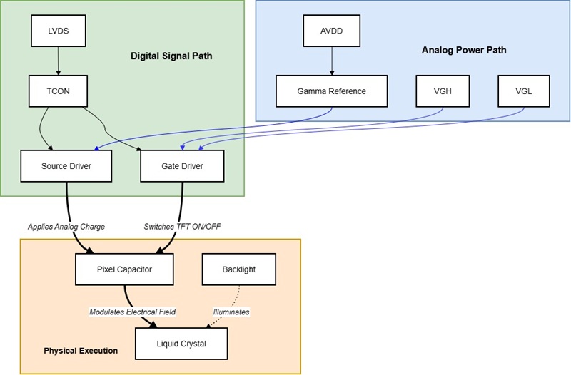
1. The Signal Flow
LVDS ➔ TCON ➔ Source/Gate Drivers
2. The Analog Bias Flow
- AVDD ➔ Gamma Reference ➔ Source Driver (Grayscale Voltage)
- VGH / VGL ➔ Gate Driver (TFT Switching)
3. The Electro-Optical Result
Gate Driver (ON) + Source Driver (Voltage) ➔ Pixel Storage Capacitor ➔ Liquid Crystal Alignment ➔ Backlight Transmission
Case Study: Powering the LMT070DNCFWD (Raw Panel Architecture)
This 7 inch TFT display module requires the host system to individually sequence the digital logic, analog reference, and both positive and negative gate-drive voltages to prevent catastrophic DC polarization or latch-up.
- Digital Logic and TFT Clamping: The sequence initiates by applying the logic power (DVDD). The DVDD slew rate (t0) must not exceed 20ms. Crucially, the negative gate-off voltage (VGL) must be applied either simultaneously with DVDD or immediately after (t3 ≥ 0ms). This is a hardware mandate to ensure the TFTs are actively clamped into a non-conducting state before any high voltages are present.
- Hardware Reset: The global Reset pin must be driven high at least 1ms (t1 > 1ms) after DVDD stabilizes to initialize the digital circuitry.
- Analog and Gate-High Assertion: A strict hardware delay of at least 16ms (t2 > 16ms) must be observed after DVDD stabilizes before the host PMIC applies the analog power (AVDD) and the gate-on voltage (VGH). Applying VGH before VGL and DVDD are stable is strictly prohibited.
- Video Signal Transmission: Only after all power rails (DVDD, VGL, AVDD, and VGH) are fully established and stable can the host MCU/MPU begin transmitting the RGB signal data, Horizontal Sync (HS), Vertical Sync (VS), and Data Enable (DE).

Q&A
Q: Can I drive the TFT backlight directly from a 3.3V or 5V GPIO pin on my host MCU?
A: No. The backlight requires an active constant-current sink/driver topology, typically an external boost converter. Connecting the LED strings directly to an unregulated voltage rail or a GPIO pin will result in thermal runaway and rapid LED degradation.
Q: Why must the VGL rail be a negative voltage (-5V to -10V) instead of just connecting it to ground (0V)?
A: Liquid crystal pixels act as capacitors. A deeply negative VGL voltage is mandatory to aggressively clamp the TFT into a hard cut-off region and suppress subthreshold leakage. If VGL is simply 0V, the transistor fails to completely shut off, and charge bleeds across the source-drain junction. This leakage causes washed-out contrast, image smearing, and cross-talk between adjacent pixels.
Q: If the display is showing accurate data but exhibits severe color banding and visible switching noise, which power rail is most likely at fault?
A: The AVDD rail. Operating typically between +8V and +12V, AVDD is the primary analog supply for the source drivers and feeds the internal resistor ladder that generates the Gamma correction curves. Any ripple or switching noise on AVDD translates directly into visible display noise, banding, or color shift.
Q: What is the primary physical risk of ignoring the recommended power-on sequence and applying VGH/VGL before VDD?
A: Failing to sequence power correctly causes DC polarization. If high-voltage gate voltages or analog signals are applied before the logic and common planes are fully established, the liquid crystals are subjected to a direct current field. This causes ion migration within the fluid, leading to permanent image retention (burn-in) and irreversible physical cell damage. It can also trigger a catastrophic parasitic SCR latch-up within the CMOS driver IC.
Q: My host MCU operates at 1.8V, but the display’s Timing Controller (TCON) requires 3.3V VDD. Can I just rely on the internal clamping diodes to handle the mismatch?
A: No, you must employ robust level-shifting. Relying on internal clamping diodes introduces parasitic power pathways, which leads to unpredictable initialization states and excessive quiescent current draw.
Q: What is the purpose of VCOM, and why is it driven as an AC signal rather than a static DC reference?
A: VCOM acts as the backplane reference voltage for the liquid crystal layer. To prevent the electrochemical destruction of the liquid crystals, they must be driven with an alternating polarity (AC). VCOM provides the baseline against which the positive and negative source voltages are dynamically applied.
Conclusion
Successful industrial TFT LCD integration is less about simply supplying power and more about managing multiple interdependent voltage domains, signal integrity, and sequencing. Whether utilizing a raw panel requiring an external PMIC or a highly integrated LCD module like the LMT101GNLFWA-NND, respecting the analog physics of the display is non-negotiable. By understanding the specific roles of AVDD, VGH, and VGL, and enforcing strict power sequencing protocols, hardware teams can reduce development risk, shorten debugging time, and significantly improve the long-term reliability of their embedded displays in the field.
Ready to source a reliable display for your next hardware revision?
Stop fighting with undocumented power sequences and parasitic latch-ups. We provide industrial-grade TFT LCD modules with fully integrated bias circuitry, backed by comprehensive engineering support. [Browse our TFT LCD Portfolio] or [Contact us for project discussion]